This 22nd article in the series of “Do It Yourself: Electronics”, finally generates a 50% duty cycle waveform using IC 555.
After failing to achieve 50% duty cycle square wave, or so called symmetric square wave, using his trivial circuitry, Pugs further explored. One clear observation was that the output pin 3 is the only pin which goes both high and low, correspondingly during the charging and discharging cycle. So, not using pin 3 means that there has to be two separate paths for charging and discharging the capacitor C, meaning two separate resistors R1 & R2 similar to the initial design as in the first 555 article.
So, Pugs restarted with the same initial design, where R2 was in discharging path and R1 + R2 in the charging path. Clearly, the problem is that R2 is also in the charging path, making it non-symmetrical. The thought of “Can R2 be removed just from the charging path?”, treaded Pugs into the short circuit and open circuit properties of diodes correspondingly in their forward and reverse biases. “Yes! Why not put a diode D1 in parallel with R2, such that D1 is short (aka forward bias) in charging cycle, and it is open (aka reverse bias) in discharging cycle?”, exclaimed Pugs. Thus, R2 would be by-passed in the charging cycle and used in the discharging cycle, exactly as desired. Here’s the modified circuit, which has just clicked:
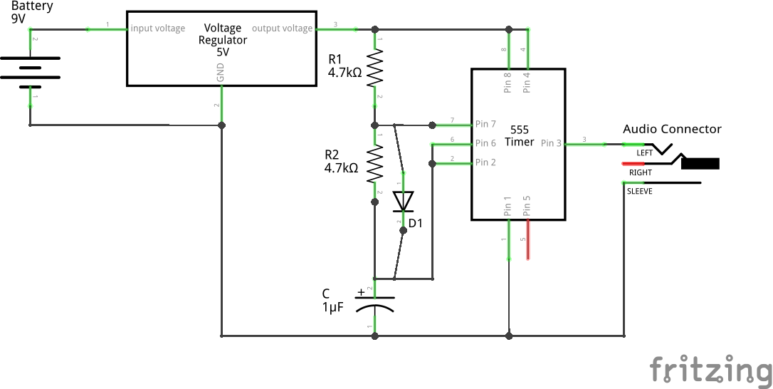
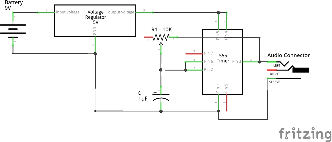
Approximate Symmetric Square Wave using 555 (Schematic)
Now the charging path has the resistor R1 & capacitor C, and the discharging path has the resistor R2 & capacitor C. So, we would get,
")
")
And if we put R1 = R2, we get a 50% duty cycle.
Live Demo
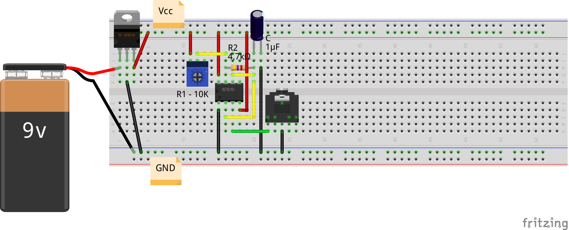
What do you think would Pugs wait for? Here’s his breadboard layout with two 4.7KΩ resistors (both of which closely measured 4.3KΩ on the multimeter), and a 1μF capacitor:

Approximate Symmetric Square Wave using 555 (Breadboard)
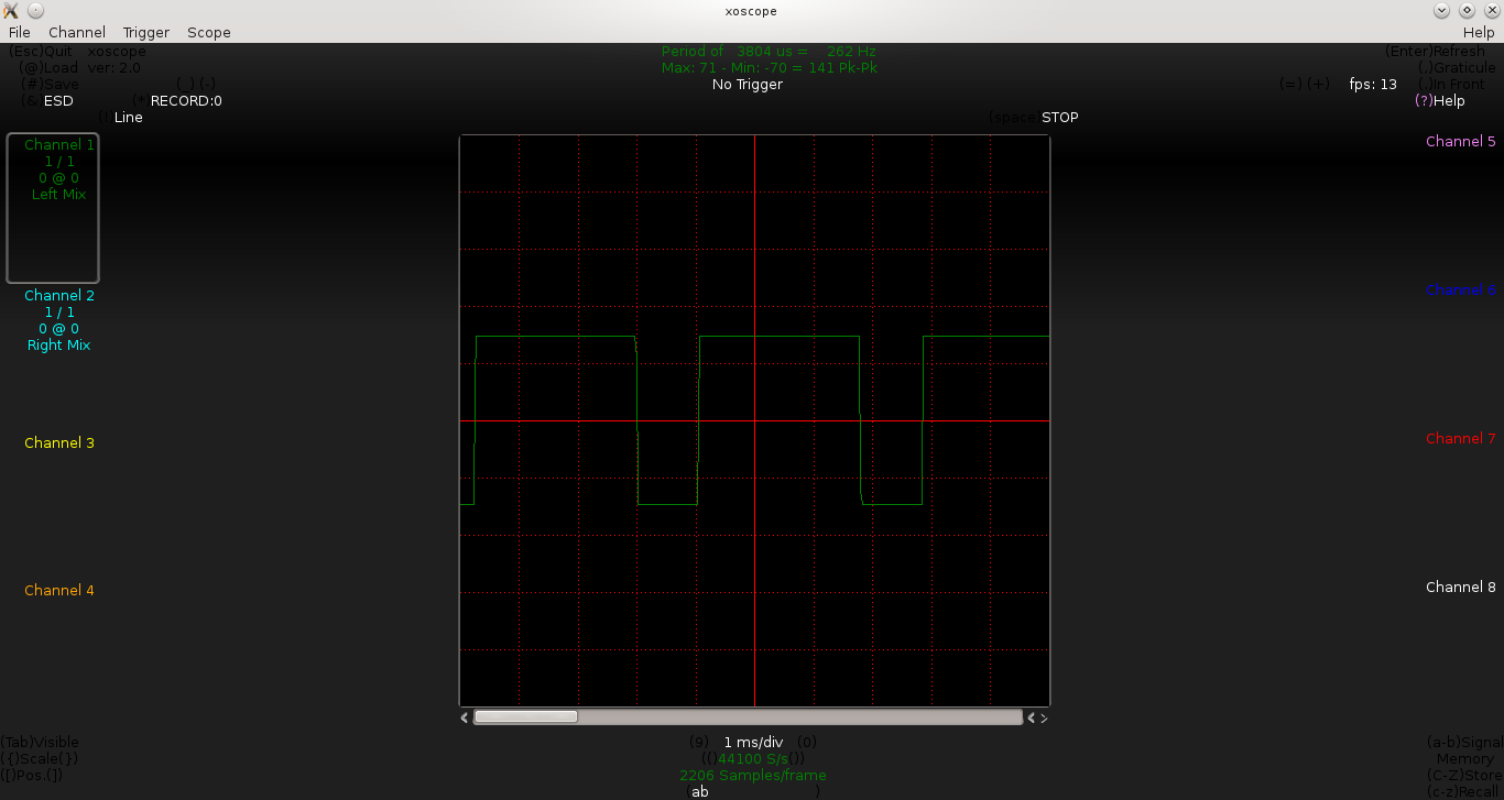
The audio jack is being used for observing the waveforms on the home-made PC oscilloscope, as created in his previous PC Oscilloscope article.
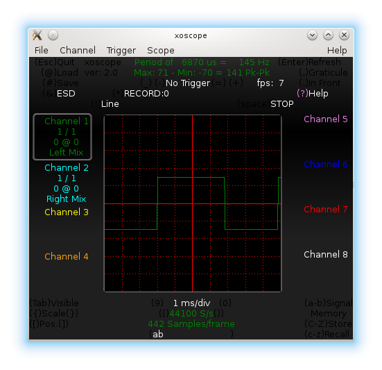
Below is the waveform observed by Pugs, for the values of R1 = R2 = 4.3KΩ (measured), and C = 1μF:
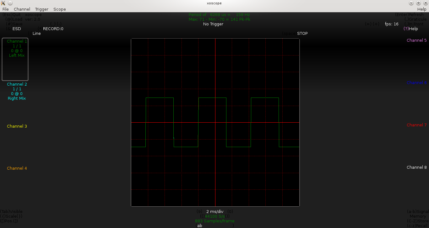
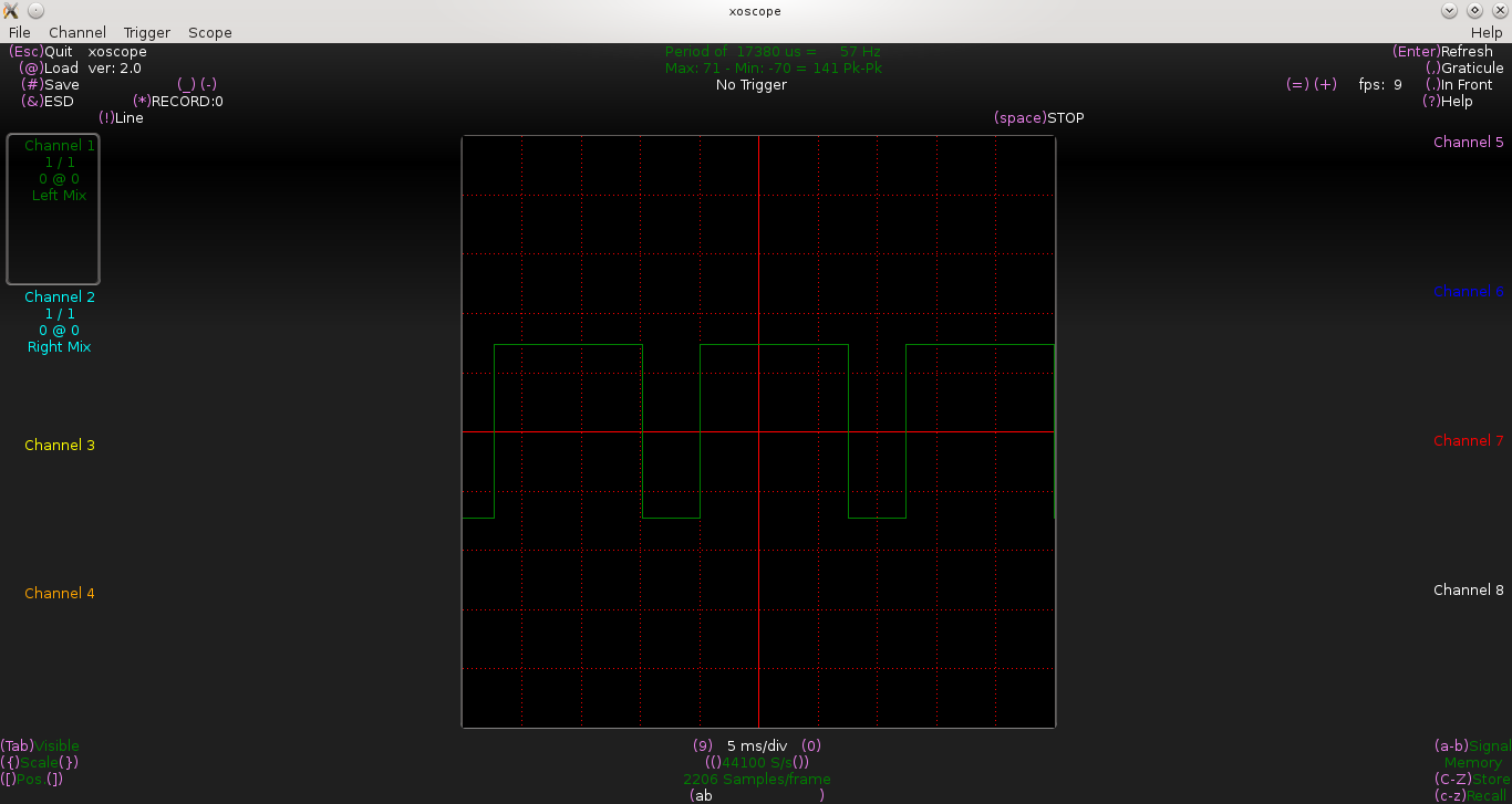
R1 = 4.3K, R2 = 4.3K, C = 1u, D1
From the above waveform, we approximately have t_on = 3.2ms and t_off = 3.0ms. Close enough to our expected value of 2.98ms (as per equation 4 or 5), but not really satisfactory as t_on and t_off are still not exactly same, even though R1 and R2 are closely equal.
In fact, t_on is slightly more, meaning the resistance in the charging path is more than just R1. O Yes! Our diode D1 is not an ideal diode, it would have some resistance in the forward bias as well, and that is what is getting added up in the charging path, causing this deviation. But how to avoid this? How about adding an equivalent diode D2 in the discharging path? That’s a cool idea, which looks like as shown below:
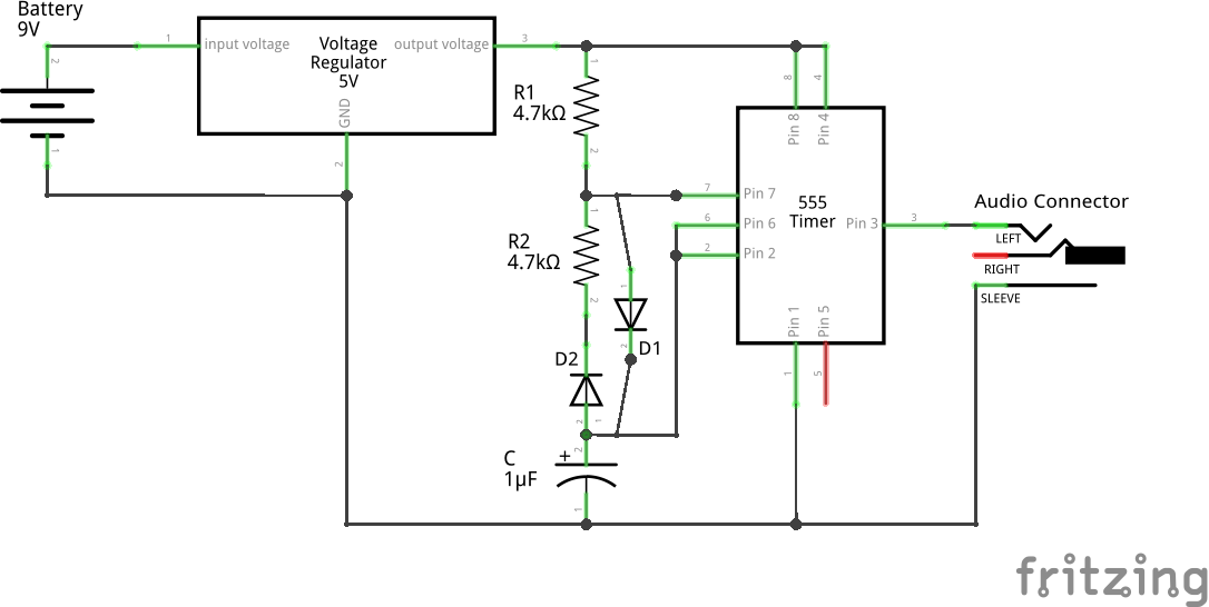
Symmetric Square Wave using 555 (Schematic)
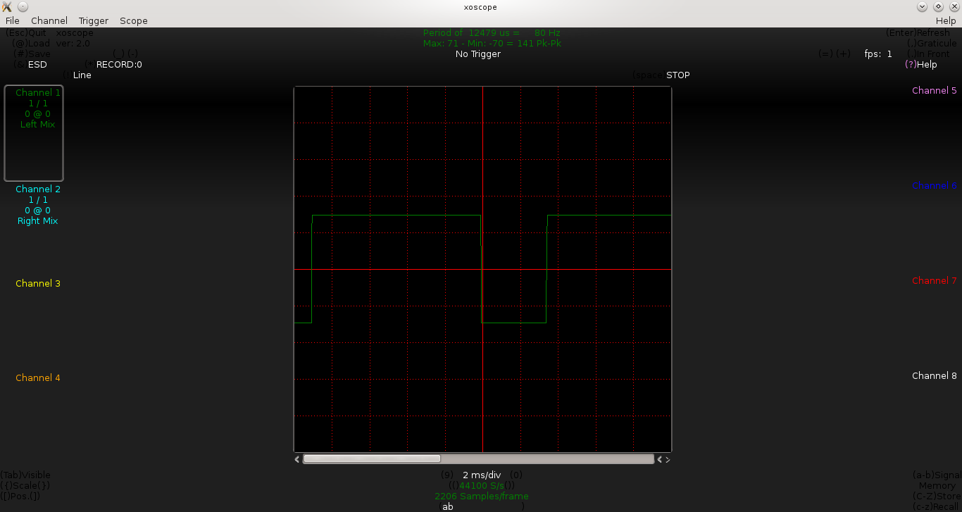
Pugs’ breadboard connections for the same are as follows:
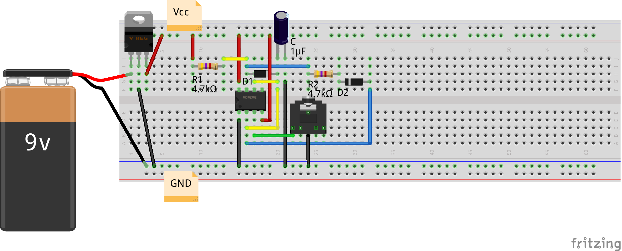
Symmetric Square Wave using 555 (Breadboard)
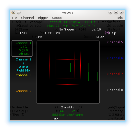
Captured waveform as follows:

R1 = 4.3K, R2 = 4.3K, C = 1u, D1, D2
And, now we see that t_on and t_off both are approximately equal to 3.2ms.
To be more exact, one may use a pot in place of R2 & D2, and then adjust it to match it with resistance of R1 & D1 – more precisely by matching the off cycle to the on cycle.
") … (3),
… (3),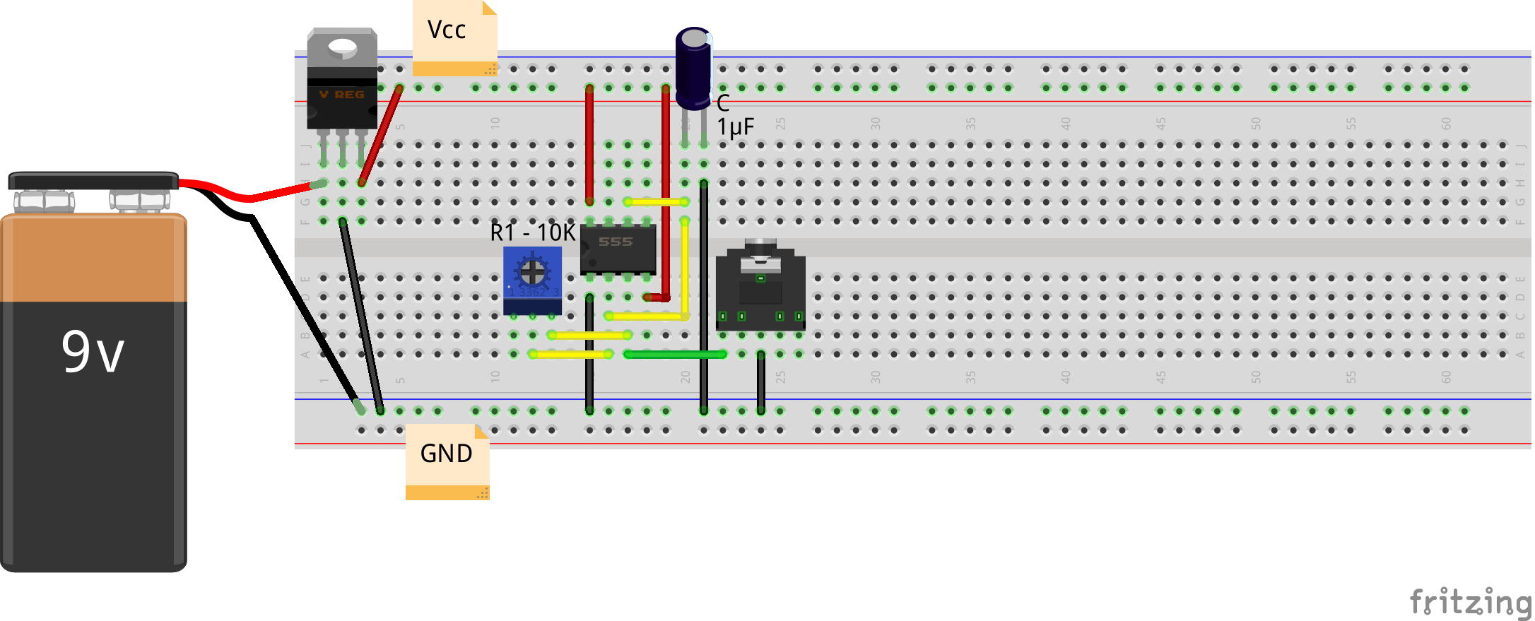
 + 1/3 * V_{cc} * e^{\frac{-t_{on}}{R*C}}") ,
, = R * C * 1.8347")

 + V_i * e^{\frac{-t}{R*C}}") ,
, + 1/3 * V_{cc} * e^{\frac{-t_{on}}{R*C}}") ,
, = (R1 + R2) * C * 0.6931") … (1)
… (1) ,
, ,
, = R2 * C * 0.6931") … (2)
… (2)