This 20th article in the series of “Do It Yourself: Electronics”, explains the basic working of IC 555 and generating a square wave using it.
<< Previous Article
Playing with raw electronics (without any microcontroller), further boosted the confidence of Pugs to dive into non-microcontroller electronics. This time he decided to explore the ever popular IC 555, loosely also known as the timer IC.
555 Functionality
555 is basically an 8-pin IC, with pin 1 for GND, pin 8 for Vcc, and pin 3 for Vo – the output voltage, which goes either high (Vcc) or low (GND), based on the other pins.
Vo goes high if the trigger pin 2 senses voltage less than 1/3 of Vcc. Vo goes low if the threshold pin 6 senses voltage greater than 2/3 of Vcc.
Pin 5 can be used as a control voltage always fixed to 2/3 of Vcc. Putting reset pin 4 low any time makes Vo go immediately low. So, if not in use it is recommended to be tied to Vcc.
Discharge pin 7 becomes GND when pin 6 senses voltage greater than 2/3 of Vcc and becomes tristate (open) when pin 2 senses voltage less than 1/3 of Vcc. In other words, discharge pin 7 becomes GND when Vo goes low and becomes open when Vo goes high.
Generating a Square Wave
Given this background, one of the common uses of the 555 IC is to generate a square wave of any particular frequency and duty cycle (on pin 3), by varying some analog voltage between GND and Vcc (on pins 2 and 6), more precisely between 1/3 Vcc and 2/3 Vcc, both inclusive. And this analog voltage is typically achieved by charging / discharging a capacitor through one or more resistors. Thus, the time constants given by τ = RC, R being the resistance, and C being the capacitance in the corresponding charging & discharging paths, controlling the corresponding on & off cycle of the square wave.
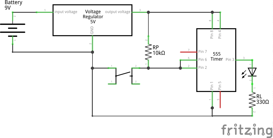
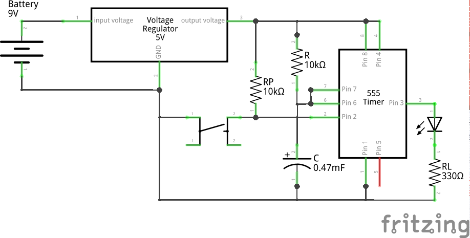
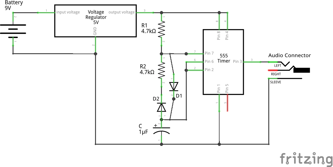
Let’s consider the following circuit with R1 as a variable resistance (pot) between 0-10KΩ, and R2 as fixed resistance of 4.7KΩ, and C as a 1μF capacitor.

Square Wave using 555 (Schematic)
In the on cycle (when Vo (pin 3) is high), pin 7 would be open. Pins 2 & 6 can be assumed tristate. Hence, then C is getting charged towards Vcc through R = R1 + R2.
In the off cycle (when Vo (pin 3) is low), pin 7 would be GND. Pins 2 & 6 can be assumed tristate. Hence, then C is getting discharged towards GND (pin 7) through R = R2.
Moreover, note that in the on cycle as soon as capacitor voltage reaches 2/3 Vcc, Vo (pin 3) becomes low, and pin 7 becomes GND, i.e. off cycle starts.
And, in the off cycle as soon as capacitor voltage drops to 1/3 Vcc, Vo (pin 3) becomes high, and pin 7 becomes tristate, i.e. on cycle starts.
And the above sequence keeps on repeating, thus giving a square wave on Vo (pin 3), with on time t_on controlled by charging through R1 + R2 and off time t_off controlled by discharging through R2.
From RC circuit analysis, we have that voltage Vc across a capacitor C, getting charged through resistance R, at time t is given by:
 + V_i * e^{\frac{-t}{R*C}}") ,
,
where Vs is supply voltage (Vcc in our case), Vi is the initial voltage on the capacitor.
So, t_on could be obtained from the fact that it starts with inital voltage Vi = 1/3 Vcc, and ends when Vc = 2/3 Vcc, being charged by Vs = Vcc through R = R1 + R2. That is,
 + 1/3 * V_{cc} * e^{\frac{-t_{on}}{R*C}}") ,
,
which on simplifying gives:
 = (R1 + R2) * C * 0.6931") … (1)
… (1)
Similarly, from RC circuit analysis, we have that voltage Vc across a capacitor C, getting discharged through resistance R, at time t is given by:
 ,
,
where Vi is the initial voltage on the capacitor.
So, t_off could be obtained from the fact that it starts with initial voltage Vi = 2/3 Vcc, and ends when Vc = 1/3 Vcc, being discharged through R = R2. That is,
 ,
,
which on simplifying gives:
 = R2 * C * 0.6931") … (2)
… (2)
Live Demo
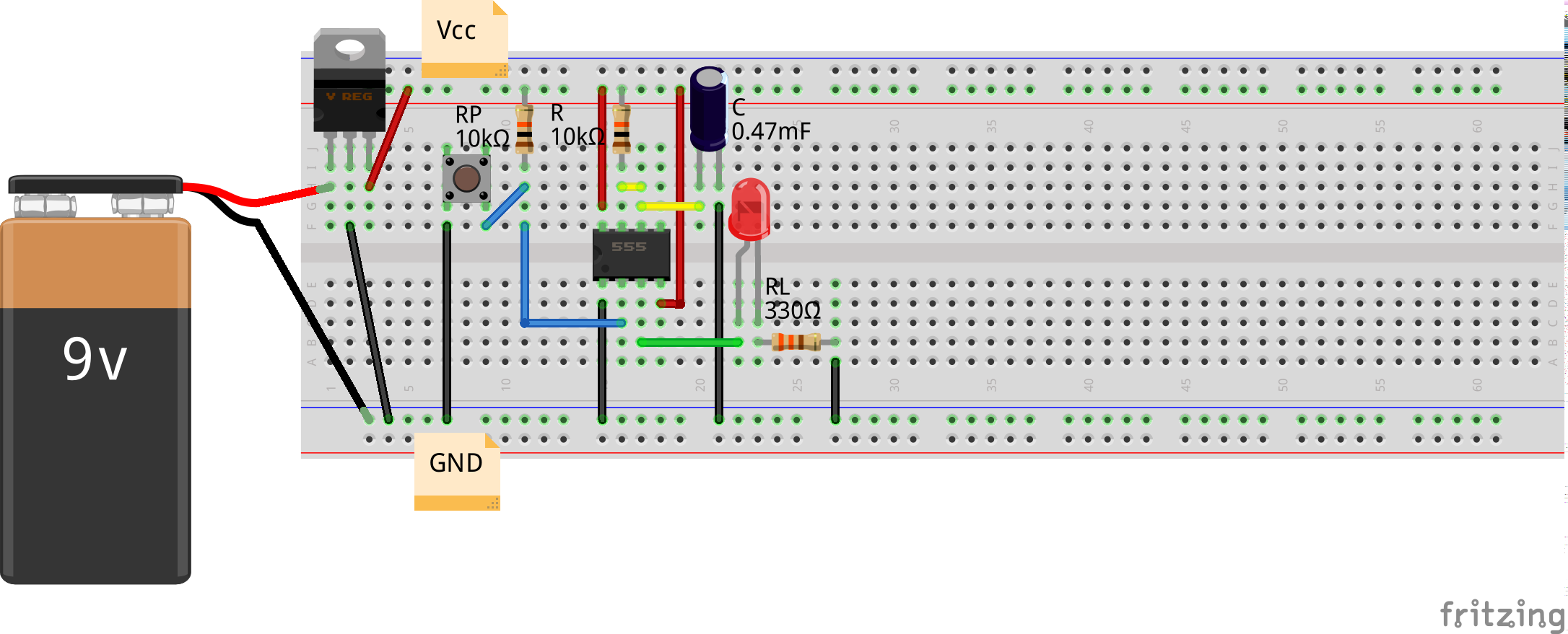
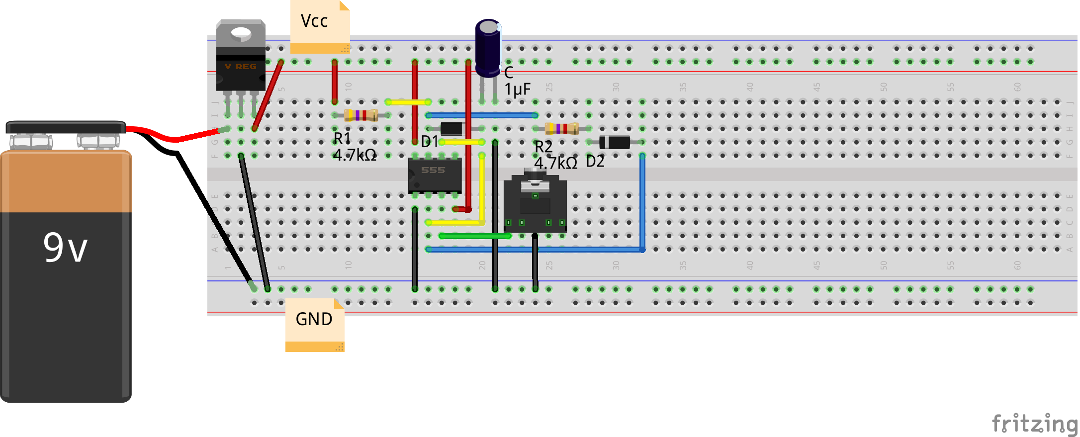
Pugs doesn’t get a punch unless he sees the theory working in practice. That’s where, he sets up the above circuitry on a breadboard as shown in the figure below:
WARNING: Do NOT put the pot to a value of zero, as that will short Vcc & GND, and may blow off the circuit. A safety workaround could be to put a fixed 1K resistor in series with the pot.
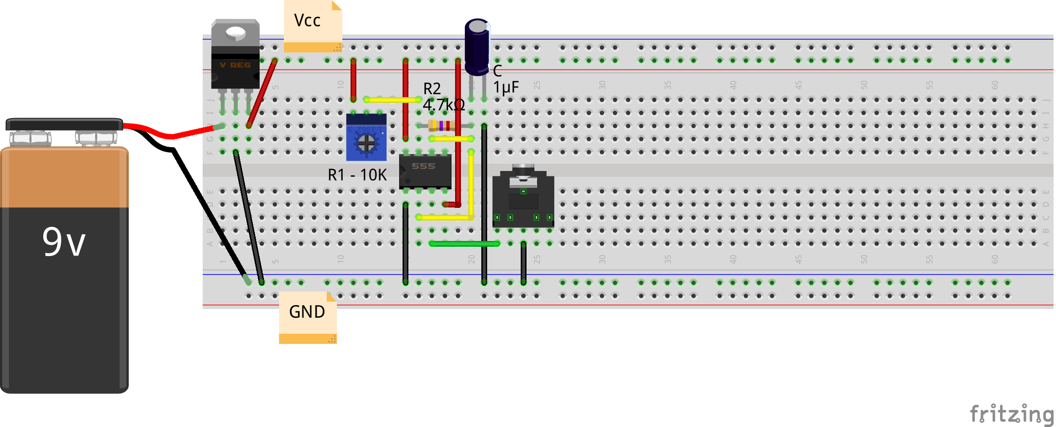
Square Wave using 555 (Breadboard)
The audio jack is being used for observing the waveforms on the home-made PC oscilloscope, as created in his previous PC Oscilloscope article.
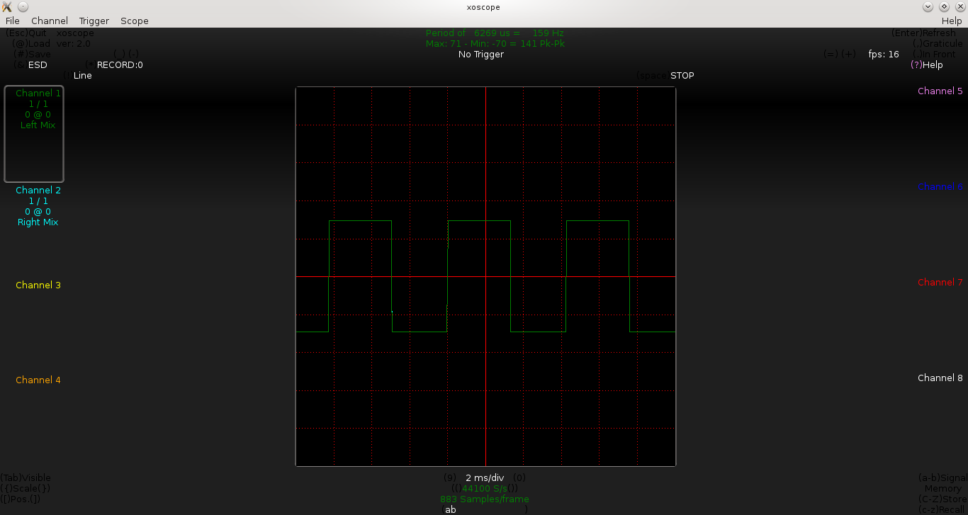
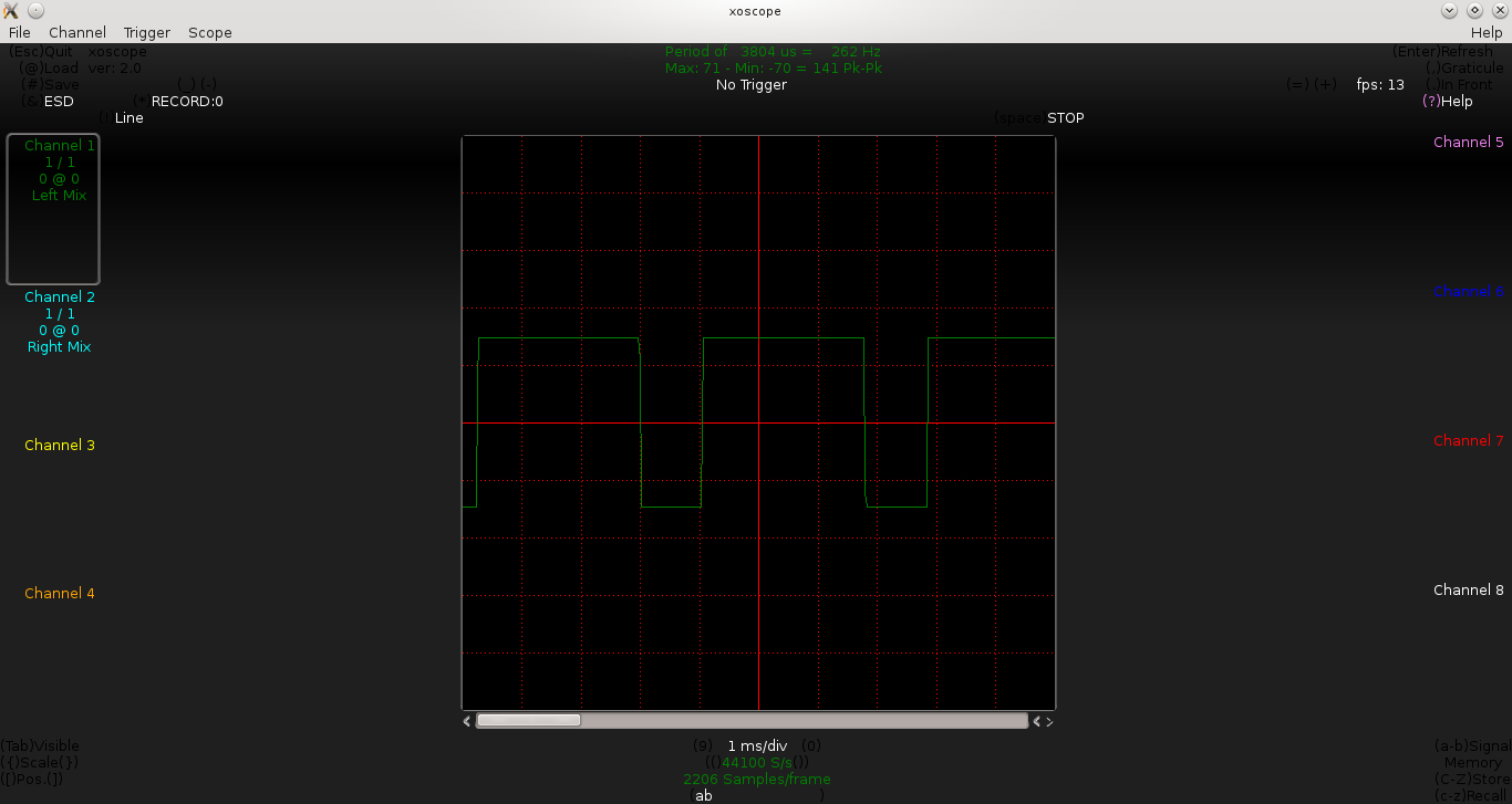
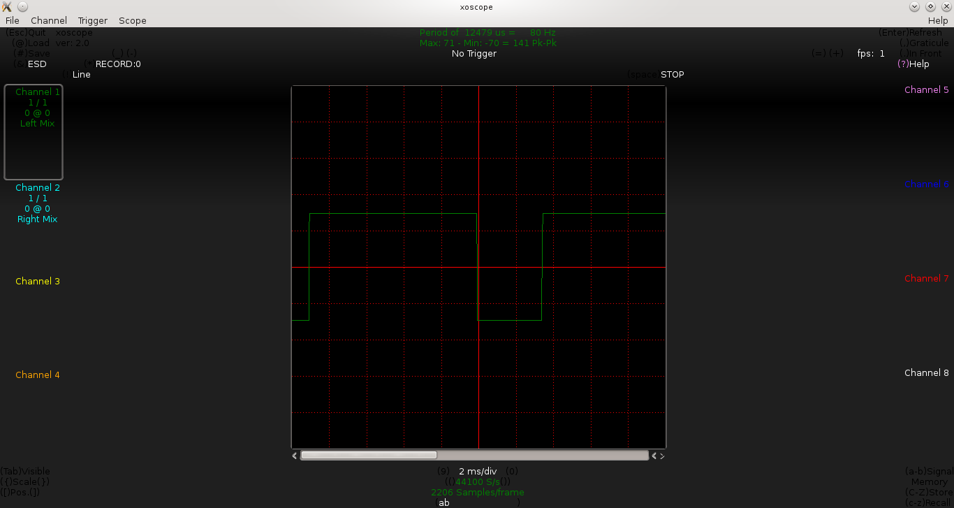
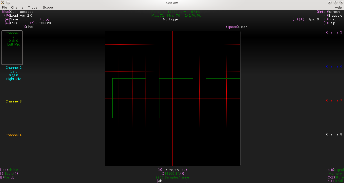
Below are the three waveforms Pugs observed for the values of R1 being adjusted to 1.28KΩ, 4.2KΩ, 8.6KΩ:
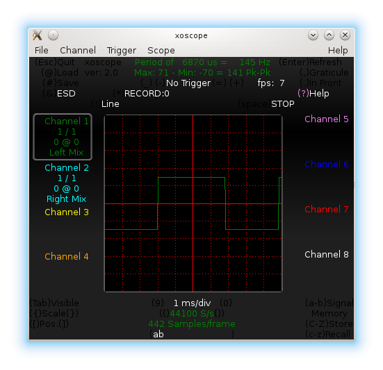
R1 = 1.28K, R2 = 4.3K
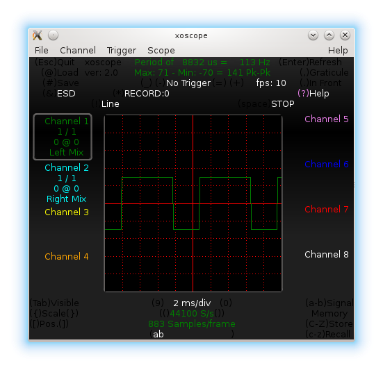
R1 = 4.15K, R2 = 4.3K
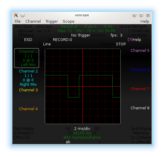
R1 = 8.60K, R2 = 4.3K
From the waveforms, Pugs approximately have the following t_on & t_off:
R1 = 1.28KΩ => t_on = 3.8ms, t_off = 3.0ms
R1 = 4.15KΩ => t_on = 6.0ms, t_off = 3.0ms
R1 = 8.60KΩ => t_on = 9.0ms, t_off = 3.0ms
Now, as per equations (1) & (2), for C = 1μF, R2 = 4.7K, and the above three R1 values, we should have got the following:
R1 = 1.28KΩ => t_on = 4.1ms, t_off = 3.3ms
R1 = 4.15KΩ => t_on = 6.1ms, t_off = 3.3ms
R1 = 8.60KΩ => t_on = 9.2ms, t_off = 3.3ms
Pretty close, but the t_off not really satisfactory. That triggered Pugs to take out his multimeter and check the resistance of the fixed resistor R2, he used. Ow! that actually measured 4.3K. Recomputing using R2 = 4.3K, gave values amazingly close to the observed values.
Summary
Thus by appropriately choosing the R1, R2, and C values one should be able to get a square wave of a desired frequency given by 1 / (t_on + t_off) and duty cycle given by t_on / (t_on + t_off). Obviously, the frequency would have a practical upper limit dictated by the 555 IC, though it is typically in MHz. What about duty cycle? Note that as per relations (1) & (2), t_on will be always greater than t_off. Thus, duty cycle would be always greater than 0.5.
So, what if we need duty cycle less than 0.5, or at least equal to 0.5, where t_on = t_off. This is what Pugs is working out on. Watch out for the next article.
Next Article >>

") … (6)
… (6)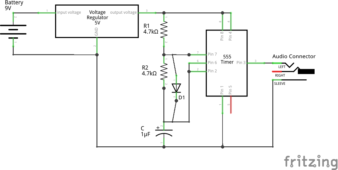
") … (4)
… (4)") … (5)
… (5)

") … (3),
… (3),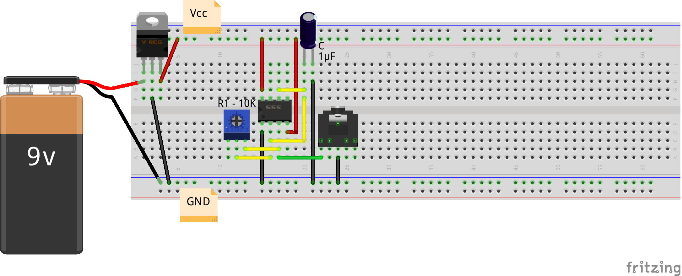
 + 1/3 * V_{cc} * e^{\frac{-t_{on}}{R*C}}") ,
, = R * C * 1.8347")