Tag Archives: basic electronics tutorial

Output Level Inversion using 555

This 24th article in the series of “Do It Yourself: Electronics”, does level inversion of a given input using IC 555.

<< Previous Article

By now, Pugs had tried two of the three operating modes of 555 – astable and monostable. How do you think, one can stop Pugs from trying the third one? So, here is his experiment to try the bistable mode, i.e. in which both high & low outputs are stable, meaning the circuit remains in the state it is in, unless triggered externally to go otherwise. A typical usage of this could be a NOT gate kind of level inversion by simply tying the input to both the trigger pin 2 and threshold pin 6.

Below is the schematic, and the breadboard connections made by Pugs with input from a pulled up switch:

Bistable (Level Inversion) using 555 (Schematic)

Bistable (Level Inversion) using 555 (Schematic)

Bistable (Level Inversion) using 555 (Breadboard)

Bistable (Level Inversion) using 555 (Breadboard)

This configuration is also referred as inverting Schmitt Trigger, and very useful in boosting fainting digital signals (though inverted) and removing noise. Putting two of such would make it non-inverting. But how does it boost or remove noise? Let’s assume Vcc = 5V. Say logic 1 (5V) signal is fainting to 4V. As it is still above 2/3 of Vcc (3.33V), the above circuitry will hit the threshold and output would be 0V (boosted logic 0). Similarly, if logic 0 (0V) is fainitng to 1V, still less than 1/3 of Vcc (1.67V), it would hit the trigger and output would be 5V (boosted logic 1). And in both cases, the output can be fed into another such circuitry to get the input boosted without inversion.

The following video clip shows the immediate output level inversion. Specifically, observe that LED is off (low output) on switch released (i.e. high input) and LED is on (high output) on switch pressed (i.e. low input).


Interestingly, the bistable output can also be obtained using two separate switches, providing a possibility of using the setup in a system, controlled by switches. Here are two possible schematics for the same:

Bistable (Schmitt Trigger Circuit 1) using 555 (Schematic)

Bistable (Schmitt Trigger Circuit 1) using 555 (Schematic)

Bistable (Schmitt Trigger Circuit 2) using 555 (Schematic)

Bistable (Schmitt Trigger Circuit 2) using 555 (Schematic)

In both the above circuits, pressing switch SH will take the Vo output high, and pressing the switch SL will take the Vo output low. The only difference being as how is the Vo output brought low – in the first one using the trigger pin 6 and in the second one using the reset pin 4.

   Send article as PDF   

Pulse Generation using 555

This 23rd article in the series of “Do It Yourself: Electronics”, generates a desired width pulse using IC 555.

<< Previous Article

After the square wave experiments, Pugs got more interested in understanding all the working modes of 555. His further studies revealed to him that 555 has basically three modes of operation:

  1. Astable – Both high & low outputs are unstable and keeps on oscillating to the other, i.e. high to low and low to high. So, also called oscillator. Examples include all the square wave generation, experimented till now, in the previous articles.
  2. Monostable – Exactly one (mono) of the outputs either high or low is a stable state. However, on an external trigger, it temporarily goes to the other unstable state, stays there for a predefined time and comes back to the stable state, on its own. This is what Pugs is planning to explore further by using a switch for the trigger. The pulse width of the unstable state is decided by the resistor and capacitor in the circuit. As it generates single (mono) pulse on trigger, it is also called monoshot configuration.
  3. Bistable – Both high & low outputs are stable, meaning the circuit remains in the state it is in, unless triggered externally to go otherwise. A typical usage of this could be a NOT gate kind of level inversion. Pugs plans to explore this in his next experimentation.

Now interestingly, the mono stability could be either in the low output or the high output. Correspondingly, the pulse would be high or low, and the trigger accordingly would be low or high. And for each of these the circuits are slightly different, especially from the perspective as to where the trigger is applied. Recall that voltage below 1/3 of Vcc on trigger pin 2 triggers output Vo pin 3 to high and voltage above 2/3 of Vcc on threshold pin 6 brings back output Vo pin 3 to low.

Below are the corresponding schematics, and the breadboard connections made by Pugs:

Monostable Low (High Pulse) using 555 (Schematic)

Monostable Low (High Pulse) using 555 (Schematic)

Monostable High (Low Pulse) using 555 (Schematic)

Monostable High (Low Pulse) using 555 (Schematic)

Monostable Low (High Pulse) using 555 (Breadboard)

Monostable Low (High Pulse) using 555 (Breadboard)

Monostable High (Low Pulse) using 555 (Breadboard)

Monostable High (Low Pulse) using 555 (Breadboard)

Observe that in either case, the trigger is being achieved on press of the switch. However, for triggering the high pulse (on Vo), Pugs needs to connect the pulled up switch output to trigger pin 2. And, for triggering the low pulse (on Vo), Pugs needs to connect the pulled down switch output to threshold pin 6. Also, note that in the first case, the final output Vo is brought back low by charging the capacitor connected to the threshold pin 6, to 2/3 of Vcc through R. And in the second case, the final output Vo is brought back high by discharging the capacitor connected to the trigger pin 2, to 1/3 of Vcc through R. And hence, in either case, the pulse width (time from trigger to restoration of stable state) would be decided by the following equation:
t_{pulse} = R * C * ln(3) … (6)
One may derive this, using the methodology similar to the one used in this previous article. So, it is left to the reader to derive the same.

Pugs tried the first (monostable at low output) experiment using two set of values: (1) R = 10KΩ, C = 100μF, (2) R = 10KΩ, C = 470μF. Using (6), the corresponding pulse widths are expected to be approximately 1 and 5 seconds.

And then he tried the second (monostable at high output) experiment using R = 10KΩ, C = 470μF. Using (6), the expected pulse width is approximately 5 seconds.

As in previous articles, Pugs tried observing the Vo output waveforms on the home-made PC oscilloscope, as created in his previous PC Oscilloscope article. But he observed nothing other than noise, except some change when he presses the switch. This reminded him that the home-made PC oscilloscope filters out low frequency (DC) voltages, and with such low frequency Vo, there would be nothing left to observe after filtering, except when there is some change on switch press. So, Pugs decided to rather use a multimeter. But, then got the idea of putting an LED instead, which is what is visible in the above circuitries.

And here are the three video clips of the LED blinkings observed in the three cases:

(1) 1 second high pulse (monostable low)


(2) 5 second high pulse (monostable low)


(3) 5 second low pulse (monostable high)


Observe the closeness of the pulse width timing (with a watch) from the above videos compared with the expected values.

Also note that during the low pulse (monostable high) experiment, Pugs is waiting for another 5+ seconds after the output Vo is high, before pressing the switch again. In fact, when he tried doing it without waiting, this is what he observed:


That’s weird – the pulse width also has reduced. But why is that? Possibly, because the capacitor is not charged back to the full, before the switch press and so it got discharged faster. That brings to the point, that derivation of equation 6 assumes that the capacitor is completely discharged in the first case (monostable low) and completely charged in the second case (monostable high), before the trigger. If not, the calculations would vary. Now, in the first case the capacitor gets immediately discharged as it is directly grounded through discharge pin 7. So, such scenario wouldn’t happen with that. However, in second case the charging is through resistors R & R1, so that would take its own time based on the RC value, which in the above case is 5+ seconds ((10 + 1)K * 470u). To avoid this, Pugs possibly would have to by-pass the big R in the charging cycle by putting a diode in parallel with R. If you believe it, go ahead and try it out.

Note: R1 has been taken small compared to R, exactly for reducing the RC effect. However, it cannot be made zero, as that would short the Vcc & GND (from discharge pin 7) when the low pulse is getting output on Vo.

Next Article >>

   Send article as PDF   

Symmetric Square Wave using 555

This 22nd article in the series of “Do It Yourself: Electronics”, finally generates a 50% duty cycle waveform using IC 555.

<< Previous Article

After failing to achieve 50% duty cycle square wave, or so called symmetric square wave, using his trivial circuitry, Pugs further explored. One clear observation was that the output pin 3 is the only pin which goes both high and low, correspondingly during the charging and discharging cycle. So, not using pin 3 means that there has to be two separate paths for charging and discharging the capacitor C, meaning two separate resistors R1 & R2 similar to the initial design as in the first 555 article.

So, Pugs restarted with the same initial design, where R2 was in discharging path and R1 + R2 in the charging path. Clearly, the problem is that R2 is also in the charging path, making it non-symmetrical. The thought of “Can R2 be removed just from the charging path?”, treaded Pugs into the short circuit and open circuit properties of diodes correspondingly in their forward and reverse biases. “Yes! Why not put a diode D1 in parallel with R2, such that D1 is short (aka forward bias) in charging cycle, and it is open (aka reverse bias) in discharging cycle?”, exclaimed Pugs. Thus, R2 would be by-passed in the charging cycle and used in the discharging cycle, exactly as desired. Here’s the modified circuit, which has just clicked:

Approximate Symmetric Square Wave using 555 (Schematic)

Approximate Symmetric Square Wave using 555 (Schematic)

Now the charging path has the resistor R1 & capacitor C, and the discharging path has the resistor R2 & capacitor C. So, we would get,
t_{on} = R1 * C * ln(2) … (4)
t_{off} = R2 * C * ln(2) … (5)

And if we put R1 = R2, we get a 50% duty cycle.

Live Demo

What do you think would Pugs wait for? Here’s his breadboard layout with two 4.7KΩ resistors (both of which closely measured 4.3KΩ on the multimeter), and a 1μF capacitor:

Approximate Symmetric Square Wave using 555 (Breadboard)

Approximate Symmetric Square Wave using 555 (Breadboard)

The audio jack is being used for observing the waveforms on the home-made PC oscilloscope, as created in his previous PC Oscilloscope article.

Below is the waveform observed by Pugs, for the values of R1 = R2 = 4.3KΩ (measured), and C = 1μF:

R1 = 4.3K, R2 = 4.3K, C = 1u, D1

R1 = 4.3K, R2 = 4.3K, C = 1u, D1

From the above waveform, we approximately have t_on = 3.2ms and t_off = 3.0ms. Close enough to our expected value of 2.98ms (as per equation 4 or 5), but not really satisfactory as t_on and t_off are still not exactly same, even though R1 and R2 are closely equal.

In fact, t_on is slightly more, meaning the resistance in the charging path is more than just R1. O Yes! Our diode D1 is not an ideal diode, it would have some resistance in the forward bias as well, and that is what is getting added up in the charging path, causing this deviation. But how to avoid this? How about adding an equivalent diode D2 in the discharging path? That’s a cool idea, which looks like as shown below:

Symmetric Square Wave using 555 (Schematic)

Symmetric Square Wave using 555 (Schematic)

Pugs’ breadboard connections for the same are as follows:

Symmetric Square Wave using 555 (Breadboard)

Symmetric Square Wave using 555 (Breadboard)

Captured waveform as follows:

R1 = 4.3K, R2 = 4.3K, C = 1u, D1, D2

R1 = 4.3K, R2 = 4.3K, C = 1u, D1, D2

And, now we see that t_on and t_off both are approximately equal to 3.2ms.

To be more exact, one may use a pot in place of R2 & D2, and then adjust it to match it with resistance of R1 & D1 – more precisely by matching the off cycle to the on cycle.

Next Article >>

   Send article as PDF   

Trivial Square Wave using 555

This 21st article in the series of “Do It Yourself: Electronics”, tries generating a 50% duty cycle waveform using a non-conventional trivial circuit using IC 555.

<< Previous Article

On further observation, of the IC 555 behaviour, Pugs got a trivial idea of generating 50% duty cycle square wave using just one resistor and one capacitor as shown in figure below:

Trivial Square Wave using 555 (Schematic)

Trivial Square Wave using 555 (Schematic)

Note that, both the charging & discharging paths would have the same resistor R & capacitor C. So, putting in the equations (1) & (2) derived in the previous article, we would get,
t_{on} = t_{off} = R * C * ln(2) … (3),
thus giving a 50% duty cycle.

Live Demo

Excited by his idea, Pugs couldn’t wait but try out the same. So, he set the above circuitry on a breadboard as shown in the figure below:

WARNING: Do NOT put the pot to a value of zero, as that will overload the circuit. A safety workaround could be to put a fixed 1K resistor in series with the pot.

Trivial Square Wave using 555 (Breadboard)

Trivial Square Wave using 555 (Breadboard)

The audio jack is being used for observing the waveforms on the home-made PC oscilloscope, as created in his previous PC Oscilloscope article.

Then, for C as a 1μF capacitor, he adjusted R to different values to get different frequencies with 50% duty cycle. But, what’s this, none of them have a 50% duty cycle.

Below are some of the waveforms being observed by Pugs, for the values of R being adjusted to 1.5KΩ, 5KΩ, 10KΩ:

R = 1.5K

R = 1.5K

R = 5K

R = 5K

R = 7K

R = 7K

From the above waveforms, we approximately have the following t_on & t_off:
R = 1.5KΩ => t_on = 2.8ms, t_off = 1.1ms
R = 5KΩ => t_on = 8.9ms, t_off = 3.4ms
R = 7KΩ => t_on = 12.5ms, t_off = 4.8ms

Now, as per equation (3), for C = 1μF, and the above three R values, we should have got the following:
R = 1.5KΩ => t_on = t_off = 1.0ms
R = 5KΩ => t_on = t_off = 3.5ms
R = 7KΩ => t_on = t_off = 4.9ms

t_offs are pretty exact, but t_ons are really high. After quite a bit of analysis, Pugs realized that the peak Vo is not actually reaching Vcc. Debugging trick he used, was to replace the 1μF capacitor by a 100μF capacitor, thus reducing the frequency in Hz (eye observable), and then measuring the Vo using a multimeter. Aha! if the Vo doesn’t reach Vcc, then in the above circuit, we are not charging the capacitor using Vcc but this measured peak value of Vo. Mathematically, this changes our derivation for equation (1) in the previous article, though equation (2) remains the same. And hence, getting a correct t_off but incorrect t_on. Even conceptually, we can see that as Vo is less than Vcc, the capacitor would take more time to charge, and thus increasing the time (t_on), as observed in all the readings above.

On this realization, Pugs approximated the measured value of maximum Vo to 3.65V, i.e. 3.65/5 of Vcc instead of Vcc in deriving the equation (1) of the previous article, getting the following relation:
2/3 * V_{cc} = 3.65/5 * V_{cc} * (1 - e^{\frac{-t_{on}}{R*C}}) + 1/3 * V_{cc} * e^{\frac{-t_{on}}{R*C}},
which on simplifying gives:
t_{on} = R * C * ln(6.2632) = R * C * 1.8347

Putting in the values, gave t_on values amazingly close to the observed values, thus again verifying the theory.

Summary

Also from the 555 IC datasheet, Pugs found that there is always some expected drop on the peak Vo from the supply voltage Vcc, and the peak Vo in most cases would be less than Vcc – thus rendering all our standard calculations of t_on futile. In fact, if we put the actual value of peak Vo in our calculations, we would get the results as observed. But getting the actual value of Vo is non-trivial and non-standard. Moreover, even if we do that somehow, we are not going to get our desired 50% duty cycle.

Thus, moral of the story is that, in general, Vo should not be used to generate the trigger voltages, as practically it may not be reaching Vcc, as in the case above. And, Pugs would have to find out some other way to achieve 50% duty cycle.

Next Article >>

   Send article as PDF   

Square Wave using 555

This 20th article in the series of “Do It Yourself: Electronics”, explains the basic working of IC 555 and generating a square wave using it.

<< Previous Article

Playing with raw electronics (without any microcontroller), further boosted the confidence of Pugs to dive into non-microcontroller electronics. This time he decided to explore the ever popular IC 555, loosely also known as the timer IC.

555 Functionality

555 is basically an 8-pin IC, with pin 1 for GND, pin 8 for Vcc, and pin 3 for Vo – the output voltage, which goes either high (Vcc) or low (GND), based on the other pins.

Vo goes high if the trigger pin 2 senses voltage less than 1/3 of Vcc. Vo goes low if the threshold pin 6 senses voltage greater than 2/3 of Vcc.

Pin 5 can be used as a control voltage always fixed to 2/3 of Vcc. Putting reset pin 4 low any time makes Vo go immediately low. So, if not in use it is recommended to be tied to Vcc.

Discharge pin 7 becomes GND when pin 6 senses voltage greater than 2/3 of Vcc and becomes tristate (open) when pin 2 senses voltage less than 1/3 of Vcc. In other words, discharge pin 7 becomes GND when Vo goes low and becomes open when Vo goes high.

Generating a Square Wave

Given this background, one of the common uses of the 555 IC is to generate a square wave of any particular frequency and duty cycle (on pin 3), by varying some analog voltage between GND and Vcc (on pins 2 and 6), more precisely between 1/3 Vcc and 2/3 Vcc, both inclusive. And this analog voltage is typically achieved by charging / discharging a capacitor through one or more resistors. Thus, the time constants given by τ = RC, R being the resistance, and C being the capacitance in the corresponding charging & discharging paths, controlling the corresponding on & off cycle of the square wave.

Let’s consider the following circuit with R1 as a variable resistance (pot) between 0-10KΩ, and R2 as fixed resistance of 4.7KΩ, and C as a 1μF capacitor.

Square Wave using 555 (Schematic)

Square Wave using 555 (Schematic)

In the on cycle (when Vo (pin 3) is high), pin 7 would be open. Pins 2 & 6 can be assumed tristate. Hence, then C is getting charged towards Vcc through R = R1 + R2.

In the off cycle (when Vo (pin 3) is low), pin 7 would be GND. Pins 2 & 6 can be assumed tristate. Hence, then C is getting discharged towards GND (pin 7) through R = R2.

Moreover, note that in the on cycle as soon as capacitor voltage reaches 2/3 Vcc, Vo (pin 3) becomes low, and pin 7 becomes GND, i.e. off cycle starts.

And, in the off cycle as soon as capacitor voltage drops to 1/3 Vcc, Vo (pin 3) becomes high, and pin 7 becomes tristate, i.e. on cycle starts.

And the above sequence keeps on repeating, thus giving a square wave on Vo (pin 3), with on time t_on controlled by charging through R1 + R2 and off time t_off controlled by discharging through R2.

From RC circuit analysis, we have that voltage Vc across a capacitor C, getting charged through resistance R, at time t is given by:
V_c = V_s * (1 - e^{\frac{-t}{R*C}}) + V_i * e^{\frac{-t}{R*C}},
where Vs is supply voltage (Vcc in our case), Vi is the initial voltage on the capacitor.

So, t_on could be obtained from the fact that it starts with inital voltage Vi = 1/3 Vcc, and ends when Vc = 2/3 Vcc, being charged by Vs = Vcc through R = R1 + R2. That is,
2/3 * V_{cc} = V_{cc} * (1 - e^{\frac{-t_{on}}{R*C}}) + 1/3 * V_{cc} * e^{\frac{-t_{on}}{R*C}},
which on simplifying gives:
t_{on} = R * C * ln(2) = (R1 + R2) * C * 0.6931 … (1)

Similarly, from RC circuit analysis, we have that voltage Vc across a capacitor C, getting discharged through resistance R, at time t is given by:
V_c = V_i * e^{\frac{-t}{R*C}},
where Vi is the initial voltage on the capacitor.

So, t_off could be obtained from the fact that it starts with initial voltage Vi = 2/3 Vcc, and ends when Vc = 1/3 Vcc, being discharged through R = R2. That is,
1/3 * V_{cc} = 2/3 * V_{cc} * e^{\frac{-t_{off}}{R*C}},
which on simplifying gives:
t_{off} = R * C * ln(2) = R2 * C * 0.6931 … (2)

Live Demo

Pugs doesn’t get a punch unless he sees the theory working in practice. That’s where, he sets up the above circuitry on a breadboard as shown in the figure below:

WARNING: Do NOT put the pot to a value of zero, as that will short Vcc & GND, and may blow off the circuit. A safety workaround could be to put a fixed 1K resistor in series with the pot.

Square Wave using 555 (Breadboard)

Square Wave using 555 (Breadboard)

The audio jack is being used for observing the waveforms on the home-made PC oscilloscope, as created in his previous PC Oscilloscope article.

Below are the three waveforms Pugs observed for the values of R1 being adjusted to 1.28KΩ, 4.2KΩ, 8.6KΩ:

R1 = 1.28K, R2 = 4.3K

R1 = 1.28K, R2 = 4.3K

R1 = 4.15K, R2 = 4.3K

R1 = 4.15K, R2 = 4.3K

R1 = 8.60K, R2 = 4.3K

R1 = 8.60K, R2 = 4.3K

From the waveforms, Pugs approximately have the following t_on & t_off:
R1 = 1.28KΩ => t_on = 3.8ms, t_off = 3.0ms
R1 = 4.15KΩ => t_on = 6.0ms, t_off = 3.0ms
R1 = 8.60KΩ => t_on = 9.0ms, t_off = 3.0ms

Now, as per equations (1) & (2), for C = 1μF, R2 = 4.7K, and the above three R1 values, we should have got the following:
R1 = 1.28KΩ => t_on = 4.1ms, t_off = 3.3ms
R1 = 4.15KΩ => t_on = 6.1ms, t_off = 3.3ms
R1 = 8.60KΩ => t_on = 9.2ms, t_off = 3.3ms

Pretty close, but the t_off not really satisfactory. That triggered Pugs to take out his multimeter and check the resistance of the fixed resistor R2, he used. Ow! that actually measured 4.3K. Recomputing using R2 = 4.3K, gave values amazingly close to the observed values.

Summary

Thus by appropriately choosing the R1, R2, and C values one should be able to get a square wave of a desired frequency given by 1 / (t_on + t_off) and duty cycle given by t_on / (t_on + t_off). Obviously, the frequency would have a practical upper limit dictated by the 555 IC, though it is typically in MHz. What about duty cycle? Note that as per relations (1) & (2), t_on will be always greater than t_off. Thus, duty cycle would be always greater than 0.5.

So, what if we need duty cycle less than 0.5, or at least equal to 0.5, where t_on = t_off. This is what Pugs is working out on. Watch out for the next article.

Next Article >>

   Send article as PDF   

Decoding an R C Circuit

This 19th article in the series of “Do It Yourself: Electronics”, decodes the working of an RC circuit.

<< Previous Article

In the previous article, Pugs understood the resistor and capacitor from a high level perspective and used some formulae to design various filters. Are you wondering, how did Pugs get those formulae? He computed them using the complex notation of the impedance of resistor R & capacitor C. Alongwith, he also used the “A * e^(j * φ)” notation for amplitute A and phase angle φ. Pugs detailed out his computations in a set of slides. Check them out below:

After the derivation of the formulae, slide 8 above shows their usage. It predicts the change in sine wave amplitude & phase angle at 2 different frequencies of 1KHz & 2KHz compared to the input, for various pairs of R & C values. And, then Pugs verifies them (within tolerance limits) by comparing the input and output waveforms, on the home-made PC oscilloscope, as created in his previous PC Oscilloscope article. Note that, while measuring, the GND is kept common for the two waveforms. Also, Pugs used the two stereo lines of the audio jack for the two waveforms, and configured xoscope accordingly.

Continuing from the previous formulae derivations, the final slide 9 shows the high-pass & low-pass filter computations and the calculation of the cut-off frequency, which has been used in the previous article.

Next Article >>

   Send article as PDF   

Basic Filter Design

This 18th article in the series of “Do It Yourself: Electronics”, demonstrates basic resistor-capacitor (RC) based filter design.

<< Previous Article

Though Pugs got the various waveforms generated, on closer look he realized that there were steps in the waveforms like sine, triangular, …. Expected right? Because of the approximation. Also, the PWM carrier frequency was present. So, would it produce the results as expected in an resistor-capacitor (RC) experiment with a single frequency sine wave? That was a big question. Or rather, can the unwanted frequencies be eliminated? That brought Pugs to the exploration of filters. Let’s see what Pugs learnt about them.

High Level understanding

Current i through a capacitor of C farads is given by C dv/dt. And if the voltage is DC that is constant, dv/dt is zero and hence i is zero. So it is said, DC is blocked by a capacitor. If the voltage is AC that is sine wave of a particular frequency, dv/dt would become a cosine wave, or sine wave with 90° phase shift but with same frequency. Along with, C becomes the multiplication factor to give C dv/dt as the non-zero current i, hence AC is allowed to pass through a capacitor.

Current i through a resistor of R ohms is given by v / R. So, AC or DC both currents are allowed through it without any phase shift, just with the multiplication factor of 1 / R.

However, combining the two (C & R) in series with a voltage input (as shown in figure below) gives very interesting results as then the current i is being controlled by both the capacitor and the resistor. Phase shift gets pulled to something between 0° and 90°. And the amplitude turns out to be attenuating depending on the sine wave frequency, with the following relation:

Amplification = \frac{\omega * R * C}{\sqrt{1 + {(\omega * R * C)}^{2}}}, where ω = 2 * π * frequency

Capacitor Resistor Series Circuit - High Pass Filter

Capacitor Resistor Series Circuit – High Pass Filter

Filter Design

Now in the amplification formula, observe that the minimum amplification is zero at zero frequency i.e. at DC, and keeps on increasing with frequency, reaching one, at infinite frequency. But practically, one can’t reach infinity. Hence, for practical purposes, the amplification is considered good enough at a value of 1/√2, which happens when ω * R * C = 1, meaning at frequency = 1/(2 * π * R * C}, which is often referred as the cut-off frequency. And for practical purposes, the currents of frequencies below this are cut-off, only allowing the ones above it. Note that, by controlling the values of R & C, one can beautifully control the cut-off frequency.

Now, this current passing through the resistor R gives the voltage vR across the resistor as R * i. Thus, this voltage also follows the same cut-off. So, if one considers the voltage v as input and the voltage vR as output, that gives a high pass filter (HPF), which passes the frequencies above the cut-off and (practically) blocks the ones below it.

Interestingly enough, if the positions of R & C are swapped (as shown in figure below), and the voltage vC across the capacitor is considered as output, it would become a low pass filter (LPF), which passes the frequencies below the cut-off and (practically) blocks the ones above it. Why? Because the amplification factor there is as follows:

Amplification = \frac{1}{\sqrt{1 + {(\omega * R * C)}^{2}}}, where ω = 2 * π * frequency

With this, Pugs have got the two simplest RC filters.

Resistor Capacitor Series Circuit - Low Pass Filter

Resistor Capacitor Series Circuit – Low Pass Filter

Filter Application

Now, for proper sine wave, most importantly Pugs wanted to remove the PWM carrier frequency, which is way higher than his various waveform frequencies of 1 & 2 KHz. So, Pugs would need a low pass filter, which passes 1KHz, 2KHz but filters out the high PWM carrier frequency. A 5KHz cut-off frequency for the filter seems okay. So, let’s compute the values of R & C for it. As per the formula, R * C = 1/(2* π * frequency) = 1/(2* π * 5000) = 31.831 * 10-6s. Assuming a value of 1K ohms for R, C could be chosen as the standard 33 nano farads. Using these two selections, Pugs computed back the cut-off frequency, which turned out to be 4.8KHz – that’s fine for Pugs.

Taking a 1K resistor and a 33 nF capacitor, Pugs connected them in series across his sine wave output.

Pugs then checked the output between RC joint and GND, on the home-made PC oscilloscope, as created in his previous PC Oscilloscope article. It showed up the sine wave as in his previous article but now with almost no carrier frequency zigzags, though the amplitude was a bit reduced.

Next Article >>

   Send article as PDF   

Micro-controller based Waveform Generator

This 17th article in the series of “Do It Yourself: Electronics”, demonstrates generating various waveforms, using the AVR micro-controller ATmega16.

<< Previous Article

Immediately after Pugs generated the 1KHz sine wave, he got the idea of generating other interesting waveforms like triangular and ramp. So, before trying some resistor-capacitor (RC) based experiments in his room, as per his plan, he first thought of just doing some more experiments with the waveforms, using his micro-controller ATmega16.

On little analysis of his code from the previous article, he realized the following:

  1. He doesn’t really need to ride these waveforms on a centred DC voltage like the sine wave
  2. And there needs to be a corresponding array containing the amplitudes for each of the waveforms

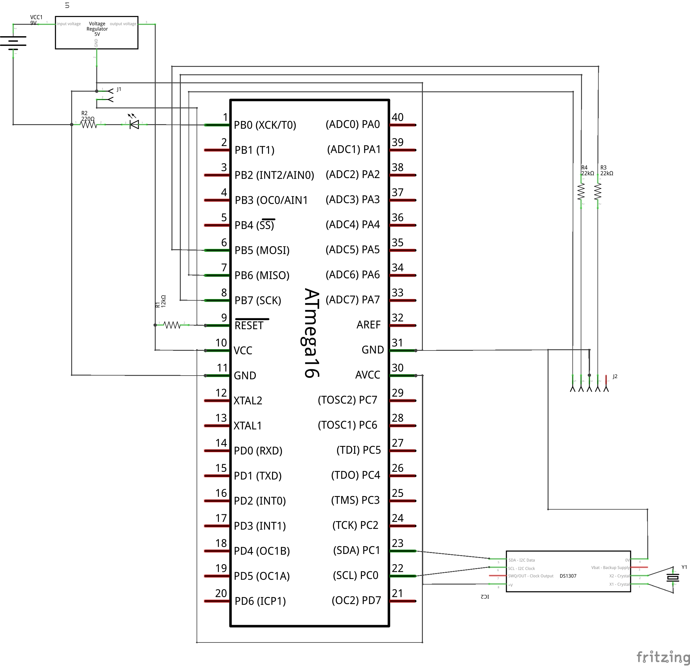
With that, he got an idea of run-time switching between the different waveforms, on say a switch press. And hence he connected a small switch to pin PB2, with its other end grounded, which he initialized to be pulled-up in the code as follows:

void init_switch(void)
{
	DDRB &= ~0b00000100; // PB2 as input
	PORTB |= 0b00000100; // Pull up on PB2
}

Now for dynamic switching, Pugs modified the function set_amplitude_centred() to work with all waveforms by taking an additional centred voltage parameter. Also, he defined an additional waveform array to contain the various waveform amplitude arrays, as follows(, so as to be able to switch between them, based on the switch press):

struct
{
	int dc_off;
	int cnt;
	int *amp;
} waveform[] =
{
	{DC_OFF, ARR_SIZE(sine), sine},
	{0, ARR_SIZE(tri_1k), tri_1k},
	{0, ARR_SIZE(tri_2k), tri_2k},
	{0, ARR_SIZE(ramp_1k), ramp_1k},
	{0, ARR_SIZE(ramp_2k), ramp_2k}
};

where sine, tri_1k, tri_2k, ramp_1k, ramp_2k are the various waveform amplitude arrays defined as follows (assuming the same interrupt cycle of 50us):

/* Length = l = 20. Period = l * 50us = 1000us = 1ms. f = 1KHz */
// 0, 18, 36, 54, 72, 90, 108, 126, 144, 162, 180, 198, 216, 234, 252, 270, 288, 306,
// 324, 342 degrees
int sine[] = {0, 3, 6, 8, 9, 10, 9, 8, 6, 3, 0, -3, -6, -8, -9, -10, -9, -8, -6, -3};
/* Length = l = 20. Period = l * 50us = 1000us = 1ms. f = 1KHz */
int tri_1k[] = {0, 1, 2, 3, 4, 5, 6, 7, 8, 9, 10, 9, 8, 7, 6, 5, 4, 3, 2, 1};
/* Length = l = 10. Period = l * 50us = 500us = 0.5ms. f = 2KHz */
int tri_2k[] = {0, 2, 4, 6, 8, 10, 8, 6, 4, 2};
/* Length = l = 20. Period = l * 50us = 1000us = 1ms. f = 1KHz */
int ramp_1k[] = {0, 1, 2, 3, 4, 5, 6, 7, 8, 9, 10, 11, 12, 13, 14, 15, 16, 17, 18, 19
		};
/* Length = l = 10. Period = l * 50us = 500us = 0.5ms. f = 2KHz */
int ramp_2k[] = {0, 1, 2, 3, 4, 5, 6, 7, 8, 9};

With all the infrastructure set, Pugs added the variable cur_wave_i for indexing the current waveform and globalized the variable i – the index into the individual amplitude arrays from the interrupt handler aka ISR. Here’s the modified switching logic in the interrupt handler:

int cur_wave_i = 0;
int i = 0;

...

ISR(TIMER0_COMP_vect)
{
	set_amplitude_centred(waveform[cur_wave_i].dc_off,
				AMP_FACTOR * waveform[cur_wave_i].amp[i]);
	if (++i == waveform[cur_wave_i].cnt)
		i = 0;
}

Note that, cur_wave_i needs to be global as would be updated from the main() based on the switch press but why has been i globalized? Think harder. And you’d realize that, as the amplitude arrays are of different sizes, the value of i could become out of array size, during switching of the array to be used on switch press. Hence, it also needs to be reset to 0, during the update of cur_wave_i. With all these changes in the previous article’s sine_wave.c code, here’s the final code as waveforms.c:

/* 
 * Generates variety of waveforms on OC2/PD7, using PWM on Timer 2.
 * Variety is generated one at a time, changing based on switch press
 * connected to PB2.
 *
 * The timing is achieved using timer interrupt handler of Timer 0 triggering
 * at a 20KHz frequency, i.e. every 50us.
 */

#include <avr/io.h>
#include <avr/interrupt.h>
#include <util/delay.h>

#define ARR_SIZE(a) (sizeof(a) / sizeof(*a))

#define PRESCALAR_BITS 0b010
#define PRESCALAR 8 // Gives 1MHz clock

#define DC_OFF 127 // Centered
#define AMP_FACTOR 5 // Should range from 1-12, for 8-bit values between 0 & 2*12*10

/* Length = l = 20. Period = l * 50us = 1000us = 1ms. f = 1KHz */
// 0, 18, 36, 54, 72, 90, 108, 126, 144, 162, 180, 198, 216, 234, 252, 270, 288, 306,
// 324, 342 degrees
int sine[] = {0, 3, 6, 8, 9, 10, 9, 8, 6, 3, 0, -3, -6, -8, -9, -10, -9, -8, -6, -3};
/* Length = l = 20. Period = l * 50us = 1000us = 1ms. f = 1KHz */
int tri_1k[] = {0, 1, 2, 3, 4, 5, 6, 7, 8, 9, 10, 9, 8, 7, 6, 5, 4, 3, 2, 1};
/* Length = l = 10. Period = l * 50us = 500us = 0.5ms. f = 2KHz */
int tri_2k[] = {0, 2, 4, 6, 8, 10, 8, 6, 4, 2};
/* Length = l = 20. Period = l * 50us = 1000us = 1ms. f = 1KHz */
int ramp_1k[] = {0, 1, 2, 3, 4, 5, 6, 7, 8, 9, 10, 11, 12, 13, 14, 15, 16, 17, 18, 19
		};
/* Length = l = 10. Period = l * 50us = 500us = 0.5ms. f = 2KHz */
int ramp_2k[] = {0, 1, 2, 3, 4, 5, 6, 7, 8, 9};

struct
{
	int dc_off;
	int cnt;
	int *amp;
} waveform[] =
{
	{DC_OFF, ARR_SIZE(sine), sine},
	{0, ARR_SIZE(tri_1k), tri_1k},
	{0, ARR_SIZE(tri_2k), tri_2k},
	{0, ARR_SIZE(ramp_1k), ramp_1k},
	{0, ARR_SIZE(ramp_2k), ramp_2k}
};

int cur_wave_i = 0;
int i = 0;

void set_amplitude_centred(uint8_t centre, uint8_t a)
{
	OCR2 = (centre + a);
}

ISR(TIMER0_COMP_vect)
{
	set_amplitude_centred(waveform[cur_wave_i].dc_off,
				AMP_FACTOR * waveform[cur_wave_i].amp[i]);
	if (++i == waveform[cur_wave_i].cnt)
		i = 0;
}

void init_pwm(void)
{
	DDRD |= 0b10000000; // PD7

	OCR2 = 0; // Initialize to 0V output

	// Setup OC2 on PD7
	TCCR2 = (1 << WGM21) | (1 << WGM20); /* Fast PWM */
	TCCR2 |= (2 << COM20); /* Clear on Match */
	TCCR2 |= (1 << CS20); /* No prescaling => Clock @ F_CPU */ // Starts the PWM
}
void init_timer(void) /* Setting Timer 0 for trigger every 50us */
{
	sei(); // Enable global interrupts
	TIMSK |= (1 << OCIE0); // Enable Compare Match interrupt
	/*
	 * Pre-scaled clock = F_CPU / PRESCALAR
	 * => Each timer counter increment takes PRESCALAR / F_CPU seconds
	 * => Formula for timer expiry interval is:
	 * 		OCR0 (top timer count) * PRESCALAR / F_CPU
	 * Example: For F_CPU = 8MHz, PRESCALAR = 8
	 * Pre-scaled clock = 8MHz / 8 = 1MHz
	 * => Each timer counter increment takes 1/1MHz = 1us
	 * => Formula for timer expiry interval is OCR0 (top timer count) * 1us
	 * Example: For 50us = OCR0 * 1us, i.e. OCR0 = 50
	 */
	OCR0 = (F_CPU / PRESCALAR) / 20000; /* 1/20000 for 50us */
	/*
	 * Setting & Starting the Timer/Counter0 in CTC (Clear Timer on Compare)
	 * (non-PWM) for controlling timer expiry interval, directly by the compare
	 * register
	 */
	TCCR0 = (1 << WGM01) | (0 << WGM00) | PRESCALAR_BITS;
}
void init_switch(void)
{
	DDRB &= ~0b00000100; // PB2 as input
	PORTB |= 0b00000100; // Pull up on PB2
}

int main(void)
{
	init_pwm();
	init_timer();
	init_switch();

	while (1)
	{
		if (!(PINB & (1 << PB2))) // Switch pressed
		{
			if (++cur_wave_i == ARR_SIZE(waveform))
			{
				i = 0; // Reset the index inside the waveform
				cur_wave_i = 0;
			}
		}
		_delay_ms(20);
	}

	return 0;
}

Then, Pugs compiled the program as follows (Note the value of F_CPU defined as 8MHz, same as in the previous article):

$ avr-gcc -mmcu=atmega16 -DF_CPU=8000000 -Os waveforms.c -o waveforms.elf
$ avr-objcopy -O ihex waveforms.elf waveforms.hex

And finally, downloaded the waveforms.hex into the ATmega16 with J1 shorted (same as in the previous articles), using the following command:

$ avrdude -c ponyser -P /dev/ttyUSB0 -p m16 -U flash:w:waveforms.hex:i

Note that Pugs have used the same ATmega16, which has been modified for 8MHz internal clock, same as in the previous article, by writing 0xE4 into the lfuse, using avrdude. Otherwise, you may have to issue the following command as well:

$ avrdude -c ponyser -P /dev/ttyUSB0 -p m16 -U lfuse:w:0xE4:m

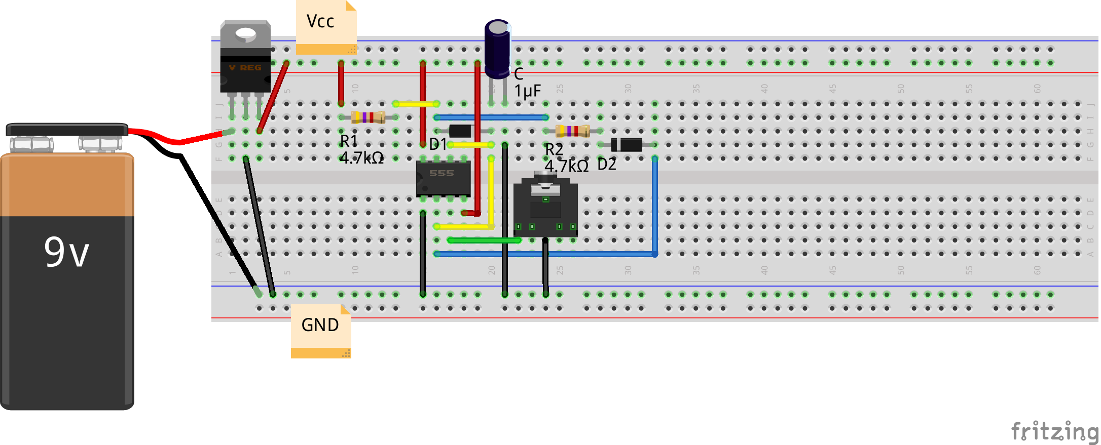
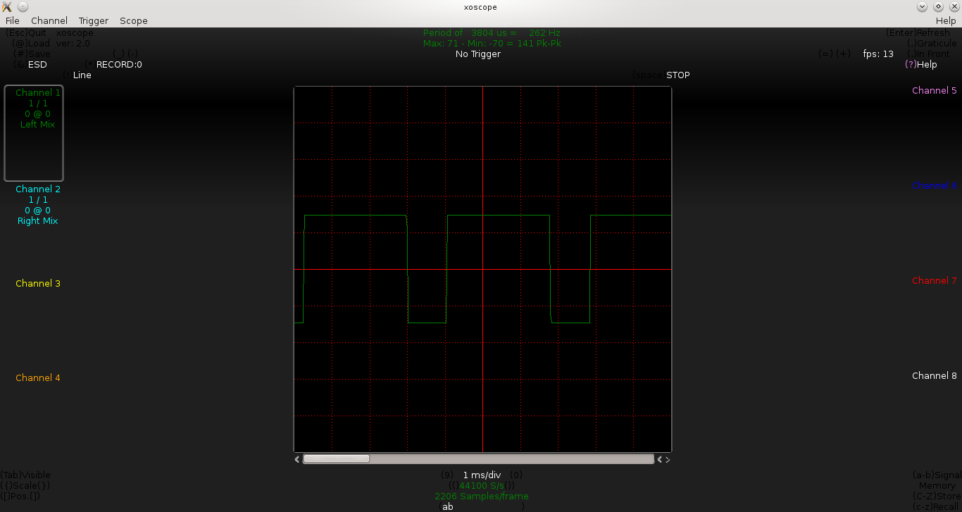
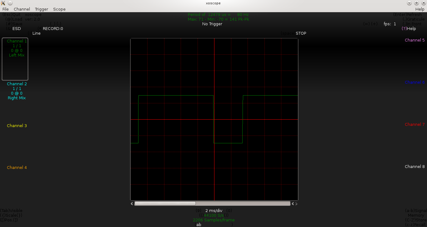
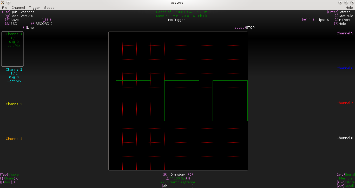
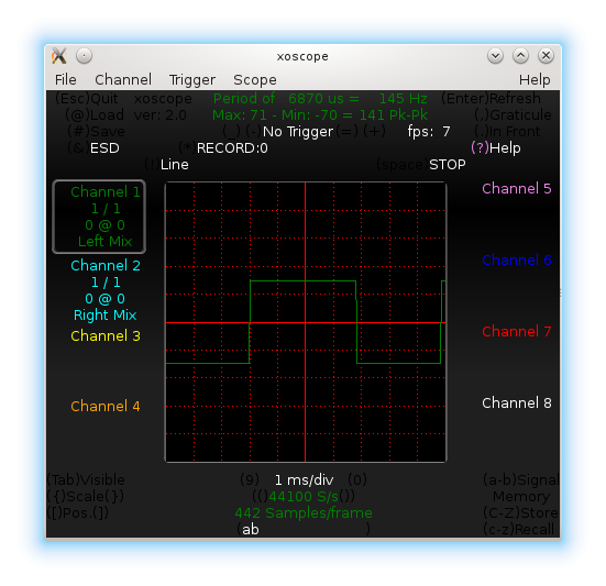
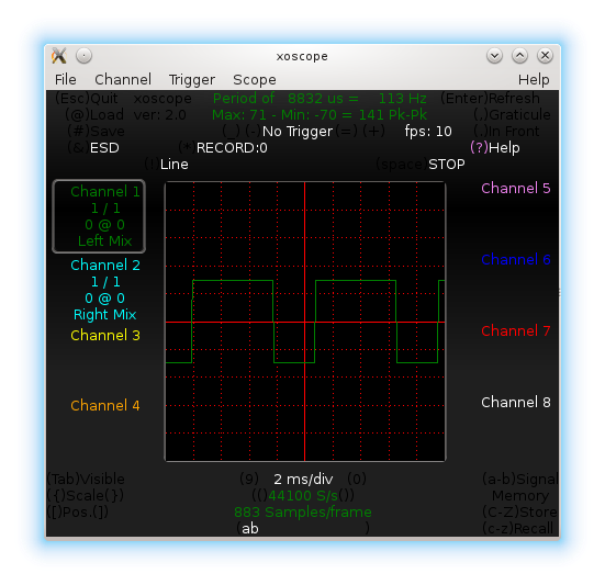
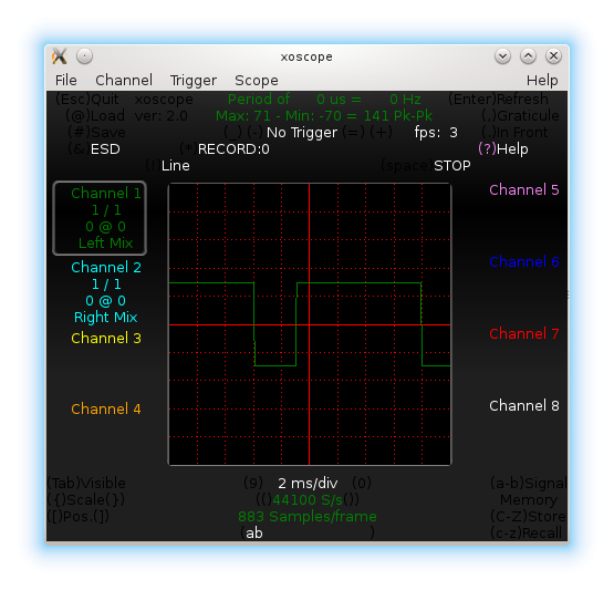
Pugs then checked the output between PD7 and GND pins of the micro-controller (after removing the short of jumper J1), on the home-made PC oscilloscope, as created in his previous PC Oscilloscope article. It showed up the sine wave exactly in the previous article. On press of the switch connected between PB2 and GND, Pugs enjoyed observing the triangular and ramp waveforms of 1 & 2 KHz, as well.

Next Article >>

   Send article as PDF   

Micro-controller based Sine Wave Generator

This 16th article in the series of “Do It Yourself: Electronics”, demonstrates generating sine wave using the AVR micro-controller ATmega16.

<< Previous Article

Pugs have been thinking of trying some resistor-capacitor (RC) based experiments in his room, the way he has done in his electronics lab. But for that he needed to have some sort of sine wave signal generator. As usual of Pugs, rather than buying a function (wave) generator, he thought of starting with creating a simple sine wave generator of his own, say at a fixed frequency of 1KHz, using his micro-controller ATmega16.

For that Pugs needed some sort of analog output generator. And, interestingly he remembered already creating a PWM-based digital to analog conversion (DAC) approximation with Rohit, in one of his previous articles. There they have generated the analog output voltage on OC0/PB3 using Timer0. However, as always, Pugs is looking for learning things he has not yet tried. So, this time, he thought of doing the analog voltage generation on OC2/PD7 using Timer2.

On deeper thought, it clicked to Pugs that for a sine wave one needs different analog outputs but in a periodic fashion. And to get a perfect periodicity, it would possibly need one more timer, say Timer0.

“So, this time why not try interrupt-based timer for the periodicity. I would also get a chance to write a interrupt handler”, flashed the thought through Pugs’ mind.

Triggered by these thoughts, here is what the initialization code written by Pugs for the Timer2 as PWM and Timer0 as 50us period timer, respectively:

#include <avr/io.h>
#include <avr/interrupt.h>

#define PRESCALAR_BITS 0b010
#define PRESCALAR 8 // Gives 1MHz clock

void init_pwm(void)
{
	DDRD |= 0b10000000; // PD7

	OCR2 = 0; // Initialize to 0V output

	// Setup OC2 on PD7
	TCCR2 = (1 << WGM21) | (1 << WGM20); /* Fast PWM */
	TCCR2 |= (2 << COM20); /* Clear on Match */
	TCCR2 |= (1 << CS20); /* No prescaling => Clock @ F_CPU */ // Starts the PWM
}
void init_timer(void) /* Setting Timer 0 for trigger every 50us */
{
	sei(); // Enable global interrupts
	TIMSK |= (1 << OCIE0); // Enable Compare Match interrupt
	/*
	 * Pre-scaled clock = F_CPU / PRESCALAR
	 * => Each timer counter increment takes PRESCALAR / F_CPU seconds
	 * => Formula for timer expiry interval is:
	 *		OCR0 (top timer count) * PRESCALAR / F_CPU
	 * Example: For F_CPU = 8MHz, PRESCALAR = 8
	 * Pre-scaled clock = 8MHz / 8 = 1MHz
	 * => Each timer counter increment takes 1/1MHz = 1us
	 * => Formula for timer expiry interval is OCR0 (top timer count) * 1us
	 * Example: For 50us = OCR0 * 1us, i.e. OCR0 = 50
	 */
	OCR0 = (F_CPU / PRESCALAR) / 20000; /* 1/20000s for 50us */
	/*
	 * Setting & Starting the Timer/Counter0 in CTC (Clear Timer on Compare)
	 * (non-PWM) for controlling timer expiry interval, directly by the compare
	 * register
	 */
	TCCR0 = (1 << WGM01) | (0 << WGM00) | PRESCALAR_BITS;
}

Obviously, Pugs referred to the ATmega16 datasheet pg 71-86 & pg 117-134. But the earlier articles on DAC and Music Generation using micro-controller were quick starters.

Computing the sine wave

Now, why is the Timer0 period set to 50us, meaning it will trigger every 50us. Let’s understand that by computing the sine wave. To generate a sine wave, one needs to output various analog voltages – theoretically speaking infinite different values between -1 to +1 multiplied by the amplitude. But practically, in our case we can make it only finite, say 20 different values. So after these 20 different values, we would repeat them, thus generating a periodic approximate sine wave. And to achieve a 1KHz sine wave, or in other words sine wave with a period of 1 / 1KHz = 1ms, we would need to output these 20 values spread over this 1ms, meaning outputting 1 value every 1ms / 20 = 50us. And, setting the Timer0 to 50us, now means outputting 1 value every time the Timer0 handler is triggered.

Time-wise computation for the sine wave done. But what about the amplitude-wise values to output during those Timer0 handler triggers. For that, note that the output on the GPIOs of a micro-controller could be only between 0V to 5V, which maps to programming the OCR2 of Timer2 between 0 to 255. Then, how do we generate negative voltages for sine wave. A usual trick applied in such scenarios is shift the 0V to the midpoint 2.5V and then oscillate the sine wave between 0 & 5V. That translates to oscillating the OCR2 values between 0 to 255 with 127 as the midpoint. Great, so for that let’s have this small handy function set_amplitude_centred():

#define DC_OFF 127 // Centred
#define AMP_FACTOR 5 // Should range from 1-12, for 8-bit values between 0 & 2*12*10

void set_amplitude_centred(uint8_t a)
{
	OCR2 = (DC_OFF + a); // DC shift by peak to get it centred around DC_OFF
}

With this, we could have the maximum sine amplitude of 127 units in terms of OCR2. So, we shall take some default, say 10, and control it by multiplying it with the AMP_FACTOR macro defined above. This allows us to have a maximum amplification factor of 12 for an amplification of 12 * 10 = 120 (< 127). Currently, just defined it to some intermediate value of 5.

All boundaries set, but what about the actual 20 values we need. For that, we have to use the sine function at intervals of 360° / 20 = 18°, i.e. \pi / 10 – the values being 0, 0.3, 0.6, 0.8, 0.9, 1.0, 0.9, 0.8, 0.6, 0.3, 0, -0.3, -0.6, -0.8, -0.9, -1.0, -0.9, -0.8, -0.6, -0.3. Multiplying by 10 (our default amplitude), we get 0, 3, 6, 8, 9, 10, 9, 8, 6, 3, 0, -3, -6, -8, -9, -10, -9, -8, -6, -3. Hence, finally we need to set the corresponding value, centred with 127, to OCR2 on every Timer2 interrupt trigger.

Programming the sine wave

Here’s the final sine_wave.c coded with an empty “while 1” in main(), as all logic is handled in the interrupt handler specified by ISR().

/* 
 * Generates sine wave @ 1KHz on OC2/PD7, using PWM on Timer 2
 *
 * The timing is achieved using timer interrupt handler of Timer 0 triggering
 * at a 20KHz frequency, i.e. every 50us.
 */

#include <avr/io.h>
#include <avr/interrupt.h>
#include <util/delay.h>

#define ARR_SIZE(a) (sizeof(a) / sizeof(*a))

#define PRESCALAR_BITS 0b010
#define PRESCALAR 8 // Gives 1MHz clock

#define DC_OFF 127 // Centred
#define AMP_FACTOR 5 // Should range from 1-12, for 8-bit values between 0 & 2*12*10

/* Length = l = 20. Period = l * 50us = 1000us = 1ms */
// 0, 18, 36, 54, 72, 90, 108, 126, 144, 162, 180, 198, 216, 234, 252, 270, 288, 306,
// 324, 342 degrees
int sine[] = {0, 3, 6, 8, 9, 10, 9, 8, 6, 3, 0, -3, -6, -8, -9, -10, -9, -8, -6, -3};

void set_amplitude_centred(uint8_t a)
{
	OCR2 = (DC_OFF + a); // DC shift by peak to get it centred around DC_OFF
}

ISR(TIMER0_COMP_vect)
{
	static int i = 0;

	set_amplitude_centred(AMP_FACTOR * sine[i]);
	if (++i == ARR_SIZE(sine))
		i = 0;
}

void init_pwm(void)
{
	DDRD |= 0b10000000; // PD7

	OCR2 = 0; // Initialize to 0V output

	// Setup OC2 on PD7
	TCCR2 = (1 << WGM21) | (1 << WGM20); /* Fast PWM */
	TCCR2 |= (2 << COM20); /* Clear on Match */
	TCCR2 |= (1 << CS20); /* No prescaling => Clock @ F_CPU */ // Starts the PWM
}
void init_timer(void) /* Setting Timer 0 for trigger every 50us */
{
	sei(); // Enable global interrupts
	TIMSK |= (1 << OCIE0); // Enable Compare Match interrupt
	/*
	 * Pre-scaled clock = F_CPU / PRESCALAR
	 * => Each timer counter increment takes PRESCALAR / F_CPU seconds
	 * => Formula for timer expiry interval is:
	 *		OCR0 (top timer count) * PRESCALAR / F_CPU
	 * Example: For F_CPU = 8MHz, PRESCALAR = 8
	 * Pre-scaled clock = 8MHz / 8 = 1MHz
	 * => Each timer counter increment takes 1/1MHz = 1us
	 * => Formula for timer expiry interval is OCR0 (top timer count) * 1us
	 * Example: For 50us = OCR0 * 1us, i.e. OCR0 = 50
	 */
	OCR0 = (F_CPU / PRESCALAR) / 20000; /* 1/20000s for 50us */
	/*
	 * Setting & Starting the Timer/Counter0 in CTC (Clear Timer on Compare)
	 * (non-PWM) for controlling timer expiry interval, directly by the compare
	 * register
	 */
	TCCR0 = (1 << WGM01) | (0 << WGM00) | PRESCALAR_BITS;
}

int main(void)
{
	init_pwm();
	init_timer();

	while (1)
	{
		_delay_ms(500);
	}

	return 0;
}

Then, Pugs compiled the program as follows (Note the value of F_CPU defined as 8MHz as in the previous article):

$ avr-gcc -mmcu=atmega16 -DF_CPU=8000000 -Os sine_wave.c -o sine_wave.elf
$ avr-objcopy -O ihex sine_wave.elf sine_wave.hex

And finally, downloaded the sine_wave.hex into the ATmega16 with J1 shorted (same as in the previous articles), using the following command:

$ avrdude -c ponyser -P /dev/ttyUSB0 -p m16 -U flash:w:sine_wave.hex:i

Note that Pugs have used the same ATmega16, which has been modified for 8MHz internal clock, as in the previous article, by writing 0xE4 into the lfuse, using avrdude. Otherwise, you may have to issue the following command as well:

$ avrdude -c ponyser -P /dev/ttyUSB0 -p m16 -U lfuse:w:0xE4:m

Pugs then checked the DC & AC voltages between PD7 and GND pins of the micro-controller, after removing the short of jumper J1. They showed up as approximately 2.5V (average) and 0.7V (root-mean-square (RMS)), respectively. And it was a visual treat to view the sine wave on the home-made PC oscilloscope, as created in his previous PC Oscilloscope article.

Next Article >>

   Send article as PDF   

Accessing the Real Time Clock

This 15th article in the series of “Do It Yourself: Electronics”, demonstrates accessing the real time clock (RTC) chip DS1307 over the I2C protocol using the AVR micro-controller ATmega16.

<< Previous Article

Equipped with I2C implementation for AVR’s ATmega16 (in the previous article), it was time to connect an I2C device to try out the protocol. Pugs decided to use the RTC chip DS1307, and then read & write the real time from it. While going through DS1307 datasheet to put it on the breadboard to connect with ATmega16, Pugs realized that he would need a 32768Hz crystal, apart from powering the RTC chip. So while purchasing the DS1307 chip, he also got the crystal.

Once ready with all the components, here is how Pugs added the RTC circuit to his existing ATmega16 programming circuit, he has been using for all his experiments till now (aka in his previous articles):

AVR RTC Interfacing Schematic

AVR RTC Interfacing Schematic

AVR RTC Interfacing Bread Board Connections

AVR RTC Interfacing Bread Board Connections

And from the DS1307 datasheet pg 7, Pugs figured out that it is the chip’s first 7 registers (for second, minute, hour, day, date, month, year in binary coded decimal (BCD) format), which need to be read or written for reading or writing the real time from the chip. Also, that the RTC operates only in standard I2C mode (pg 10) and the 7-bit slave address of the RTC is 0b1101000 (pg 12). And accordingly, he prototyped the RTC logic in rtc.h and programmed them in rtc.c.

Header rtc.h is as follows:

#ifndef RTC_H
#define RTC_H

void rtc_init(void);
int rtc_set(uint8_t y, uint8_t mo, uint8_t d, uint8_t dy, uint8_t h, uint8_t m,
		uint8_t s);
int rtc_get(uint8_t *is_halted, uint8_t *y, uint8_t *mo, uint8_t *d, uint8_t *dy,
		uint8_t *h, uint8_t *m, uint8_t *s);
int rtc_get_str(uint8_t *is_halted, char date_str[15], char time_str[9]);

#endif

And the complete implementation of rtc.c goes here (Note the usage of TWI APIs implemented in the previous article):

#include <avr/io.h>

#include "twi.h"
#include "rtc.h"

#define RTC_DEV_ADDR 0b1101000

void rtc_init(void)
{
	twi_init(standard);
}

int rtc_set(uint8_t y, uint8_t mo, uint8_t d, uint8_t dy, uint8_t h, uint8_t m,
		uint8_t s)
{
	uint8_t rtc_data[8] = { /* RTC Registers' start address */ 0x00, };
	uint8_t *rtc_reg = rtc_data + 1;

	/* RTC Registers */
	rtc_reg[0] = ((s / 10) << 4) | (s % 10); /* seconds in BCD */
	rtc_reg[1] = ((m / 10) << 4) | (m % 10); /* minutes in BCD */
	rtc_reg[2] = ((h / 10) << 4) | (h % 10); /* hours in BCD */
	rtc_reg[3] = dy; /* day in BCD : 7 for Saturday */
	rtc_reg[4] = ((d / 10) << 4) | (d % 10); /* date in BCD */
	rtc_reg[5] = ((mo / 10) << 4) | (mo % 10); /* month in BCD */
	rtc_reg[6] = ((y / 10) << 4) | (y % 10); /* year in BCD */

	return twi_master_tx(RTC_DEV_ADDR, rtc_data, sizeof(rtc_data));
}

int rtc_get(uint8_t *is_halted, uint8_t *y, uint8_t *mo, uint8_t *d, uint8_t *dy,
		uint8_t *h, uint8_t *m, uint8_t *s)
{
	int ret;
	uint8_t rtc_data = 0x00; /* RTC Registers' start address */
	uint8_t rtc_reg[7];

	if ((ret = twi_master_tx_rx(RTC_DEV_ADDR, &rtc_data, 1, rtc_reg, 7)) == 0)
	{
		*is_halted = rtc_reg[0] >> 7;
		/* seconds from BCD */
		*s = 10 * ((rtc_reg[0] >> 4) & 0x7) + (rtc_reg[0] & 0xF);
		/* minutes from BCD */
		*m = 10 * (rtc_reg[1] >> 4) + (rtc_reg[1] & 0xF);
		/* hours from BCD */
		*h = 10 * (rtc_reg[2] >> 4) + (rtc_reg[2] & 0xF);
		/* day from BCD : 7 for Saturday */
		*dy = rtc_reg[3];
		/* date from BCD */
		*d = 10 * (rtc_reg[4] >> 4) + (rtc_reg[4] & 0xF);
		/* month from BCD */
		*mo = 10 * (rtc_reg[5] >> 4) + (rtc_reg[5] & 0xF);
		/* year from BCD */
		*y = 10 * (rtc_reg[6] >> 4) + (rtc_reg[6] & 0xF);
	}
	return ret;
}

int rtc_get_str(uint8_t *is_halted, char date_str[15], char time_str[9])
/* Format Example: date_str[] = "01.06.2075 Sat"; time_str[] = "03:07:00"; */
{
	int ret;
	uint8_t rtc_data = 0x00; /* RTC Registers' start address */
	uint8_t rtc_reg[7];
	uint8_t day;
	char *day_str[] = { "", "Sun", "Mon", "Tue", "Wed", "Thu", "Fri", "Sat" }; 

	if ((ret = twi_master_tx_rx(RTC_DEV_ADDR, &rtc_data, 1, rtc_reg, 7)) == 0)
	{
		*is_halted = rtc_reg[0] >> 7;
		date_str[0] = '0' + (rtc_reg[4] >> 4);
		date_str[1] = '0' + (rtc_reg[4] & 0xF);
		time_str[2] = '.';
		date_str[3] = '0' + (rtc_reg[5] >> 4);
		date_str[4] = '0' + (rtc_reg[5] & 0xF);
		time_str[5] = '.';
		time_str[6] = '2';
		time_str[7] = '0';
		date_str[8] = '0' + (rtc_reg[6] >> 4);
		date_str[9] = '0' + (rtc_reg[6] & 0xF);
		time_str[10] = ' ';

		day = rtc_reg[3] & 0xF;
		date_str[11] = day_str[day][0];
		date_str[12] = day_str[day][1];
		date_str[13] = day_str[day][2];
		date_str[14] = 0;

		time_str[0] = '0' + (rtc_reg[2] >> 4);
		time_str[1] = '0' + (rtc_reg[2] & 0xF);
		time_str[2] = ':';
		time_str[3] = '0' + (rtc_reg[1] >> 4);
		time_str[4] = '0' + (rtc_reg[1] & 0xF);
		time_str[5] = ':';
		time_str[6] = '0' + ((rtc_reg[0] >> 4) & 0x7);
		time_str[7] = '0' + (rtc_reg[0] & 0xF);
		time_str[8] = 0;
	}
	return ret;
}

With all code set to read and write the RTC, Pugs needed some application code to call these. That’s where he implemented the following rtc_serial.c to operate on the RTC using serial interface. Yes, the same serial interface, he had setup in the previous articles, using the TTL to USB converter. Note the usage of serial APIs implemented in the previous USART article, and used in the previous debugging article, with modified serial.c.

#include <avr/io.h>
#include <util/delay.h>

#include "rtc.h"
#include "serial.h"

char date[] = "01.06.2075 Sat";
char time[] = "03:07:00";

int main(void)
{
	uint8_t is_halted;

	rtc_init();
	usart_init(9600);

	/* Initialize the clock to 2075.June.1st Sat 03:07:00 */
	if (rtc_set(75, 6, 1, 7, 3, 7, 0) == 0)
	{
		usart_tx(date);
		usart_byte_tx(' ');
		usart_tx(time);
	}
	else
	{
		usart_tx("RTC set failed. Halting ... ");
		while (1);
	}
	usart_byte_tx('\n');

	while (1)
	{
		if (rtc_get_str(&is_halted, date, time) == 0)
		{
			usart_tx(date);
			usart_byte_tx(' ');
			usart_tx(time);
		}
		else
			usart_tx("RTC read failed");
		usart_byte_tx('\n');
		_delay_ms(5000);
	}

	return 0;
}

Then, Pugs compiled all the programs together as follows (Note the value of F_CPU defined as 8MHz unlike earlier cases):

$ avr-gcc -mmcu=atmega16 -DF_CPU=8000000 -Os rtc_serial.c rtc.c twi.c serial.c -o
rtc_serial.elf
$ avr-objcopy -O ihex rtc_serial.elf rtc_serial.hex

And finally, downloaded the rtc_serial.hex into the ATmega16 with J1 shorted (same as in the previous articles), using the following command:

$ avrdude -c ponyser -P /dev/ttyUSB0 -p m16 -U flash:w:rtc_serial.hex:i

Pugs then connected the USB to TTL converter to his laptop on the USB side, and the RX, TX, GND pins of the USB to TTL converter to the TXD, RXD, GND pins of the micro-controller. And started the serial application minicom as root on his laptop as follows (same as in the previous articles):

# minicom -D /dev/ttyUSB1 -b 9600 -o

Note that Pugs’ TTL to USB connector shows up as /dev/ttyUSB1 on his laptop. In case, yours is different, use that instead. But what’s this, even after removing the jumper J1, no output on the minicom – seems like it is stuck. Aha! suddenly, it clicked to Pugs that he has missed something important, which was decided during the TWI implementation (in the previous article). Yes, the fuse settings of the ATmega16 to be changed for it to operate at 8MHz. So, that’s what exactly he did next.

As per the ATmega16 datasheet pg 260-261 & pg 29, the low fuse byte needs to be updated to 0xE4 from 0xE1, for it to operate at 8MHz clock. Hence, Pugs issued the following avrdude command with J1 shorted:

$ avrdude -c ponyser -P /dev/ttyUSB0 -p m16 -U lfuse:w:0xE4:m

And yes, this time after removing the short of jumper J1, he started getting the date & time displayed every 5 seconds from 2075. And, to quit from minicom, Pugs typed Ctrl-A Q.

Next Article >>

   Send article as PDF